
SpeedFit™ Design Simulator
Simulate and evaluate the performance of SiC-based power circuits and determine the right SiC device in seconds.
Start a SimulationC6D04065E Thermal Characteristics

Hi,
I am trying to run a thermal simulation of a board using the C6D04065E devices in Cadence's Celsius PowerDC simulator. The only thermal characteristic given in the diode datasheet is the R_JC figure, which is 2.89 C/W. The Cadence simulator has several settings for choosing thermal characteristics, see attached screenshots.
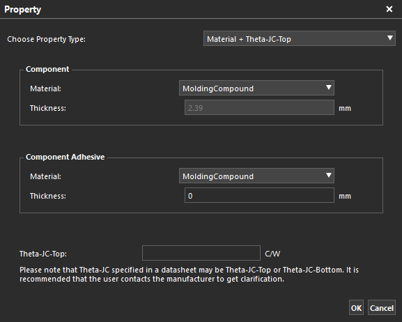
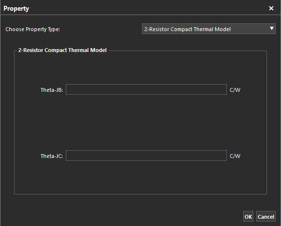
Can you provide data on the junction-board thermal resistance (or maybe guesstimate) and clarify if the junction-case number is referenced to the package top or bottom?
// Thanks
Comments
-
Thank you for your post, it has been approved and we will respond as soon as possible.
0 -
Hello aesis,
Thank you for your questions.
- The Rth,j-c from the datasheet is the thermal impedance from the junction to bottom-case of the device.
- You can estimate the case to board impedance for the E package using:
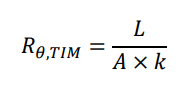
Where L is the thickness of the solder, A is the assumed thermal transfer area and k is the thermal conductivity of solder used.
Assuming a general solder thickness of 0.1mm, the approximate area of the case of E package= 25mm^2 and k for lead-tin solder to be 50 W/m.K: the Rth from case to board is 0.08 K/W.
The total Rth,j-b (junction to board) = Rth,j-c + 0.08 K/W (approximate)
You can find more details here:
Thermal Management of Bottom-Side Cooled Surface Mount Devices and Design Considerations
Let me know if you have any other questions. Thank you!
0 -
Hi TBhatia,
Thank you for your answer. For modelling completeness, do you have a number for the thermal resistance to the package top?
// Thanks
0