CGD1700HB2M-UNA Configuration
Hello,
I am developing an H-bridge using CGD1700HB2M-UNA gate driver modules and CAB016M12FM3 half-bridge MOSFET units. However, I am facing an issue with configuring the CGD1700HB2M-UNA.
The documentation mentions that a differential transceiver is required between the MCU and the CGD1700HB2M-UNA module. However, I attempted to send signals directly to the CGD1700HB2M-UNA using an MCU and observed the PWM signals, but I was unsuccessful. When I enable the PWM signals, the DT1 and DT2 LEDs start blinking.
I would like to know if it is possible to operate the gate driver module without the differential transceiver, or if it is mandatory for proper functionality. Additionally, I want to confirm whether the half-bridge module must be connected to the gate driver in order to observe the PWM signals. Currently, I am trying to observe the PWM signals without connecting the half-bridge units.
Could you please help me resolve this issue?
Thank you,
Best,
Sachith.
Comments
-
Thank you for your post, it has been approved and we will respond as soon as possible.
0 -
Hi,
I have figured out the problem with the transceiver module, and I have bought the differential transceiver module and started testing the PWM signal. However, I realized that I was not getting the PWM signal without the half-bridge module. I identified that the gate driver has an overcurrent protection feature, which immediately detects a fault because the HS-Drain connection is floating. After connecting the half-bridge module, I was able to get the PWM output.
However, I have another problem. I saw in a forum discussion (link) that the peak output current of the gate driver is mentioned. The gate driver used in the CGD1700HB2M-UNA module has a ±10A peak output current. In the module, the resistor values for the gate and source are selected as 1Ω. I am confused about the gate-to-source voltage of the gate driver output (whether it is +20V or a lower value due to the LT3082EDD#PBF regulator). If it is 20V, the peak current would be 20A (20V / 1Ω). Can you please provide an explanation for this?
Secondly, I would like to understand the effect of gate resistance on the peak current. I am using a CAB016M12FM3 half-bridge module in my setup. In the datasheet, it is mentioned that it has a 2.4Ω gate resistance. To minimize the peak current, can I consider the gate resistance of the SiC module? That is, without changing the 1Ω resistor in the gate driver module, can I calculate the peak current by summing the gate resistance and the 1Ω resistor (e.g., 20V / (1Ω + 2.4Ω))?
Looking forward to your explanation.
Thank you,
Sachith0 -
Hello Sachith,
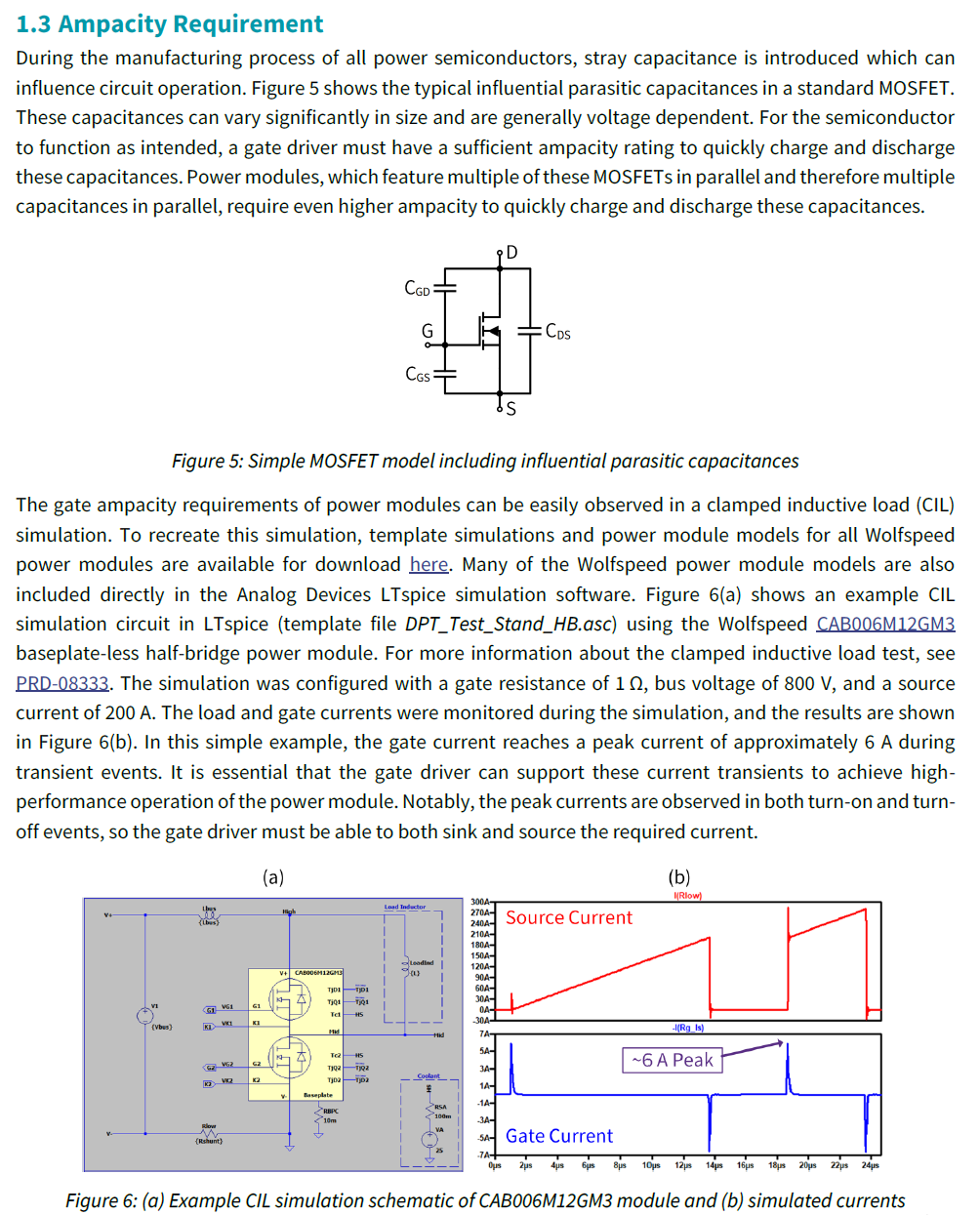
The power module only requires high output current during transient events, where the MOSFET capacitances must be charged and discharged quickly. The gate driver current rating of 10 A is the maximum possible output current which can then be reduced further through the use of external gate resistance. Please see the gate driver ampacity requirement explanation below for more information. I recommend recreating the described simulation in LTspice to understand the peak current dynamics in your system.
The links embedded in the text are listed below:
- here:
- CAB006M12GM3:
- PRD-08333:
Thanks,
Chris N.
0 -
Hi Chris,
Thank you very much for the information. I am familiar with PLECS software, and I will proceed with the simulation.
I have one other question for you:
Does Wolfspeed provide the symbol and footprint for the CAB016M12FM3 half-bridge module?Best regards,
Sachith.
0 -
Sachith,
Please note that this simulation would be better performed in a SPICE tool such as LTspice. PLECS is powerful software that excels at system-level analysis, since it can easily simultaneously model electrical, thermal, and magnetic domains. It models electrical switching dynamics as ideal switch events and references losses from a look-up table. This allows it to run full converter models quickly and efficiently. However, the instantaneous switch events used in PLECS will not demonstrate the high gate driver transient currents described in my previous post. To observe and understand that behavior, you will need to run the simulation in a SPICE simulator or similar. Wolfspeed recommends using LTspice (which is free) and has guides on how to quickly begin simulating in LTspice.
I attached the Altium footprint for the requested module. Please note that this should be used as a starting point for your design. The pin hole dimensions are intended for pressing in the module. If you plan to solder the module, the hole diameters should be increased. Additionally, this footprint includes the optional additional mounting holes. See the Wolfpack mounting guide here for more information.
Thanks,
Chris N.0 -
Hi, I hope that this answered your question. I will close this discussion for now but if you have a follow up question, please "Start a New Discussion" and we would be glad to support you further.
0

