
SpeedFit™ Design Simulator
Simulate and evaluate the performance of SiC-based power circuits and determine the right SiC device in seconds.
Start a SimulationCRD25DA12N Design

Hi
I'm currently researching different designs and came across the CRD25DA12N-FMC reference design. After reviewing its circuit, I have a few questions and would appreciate any insights.
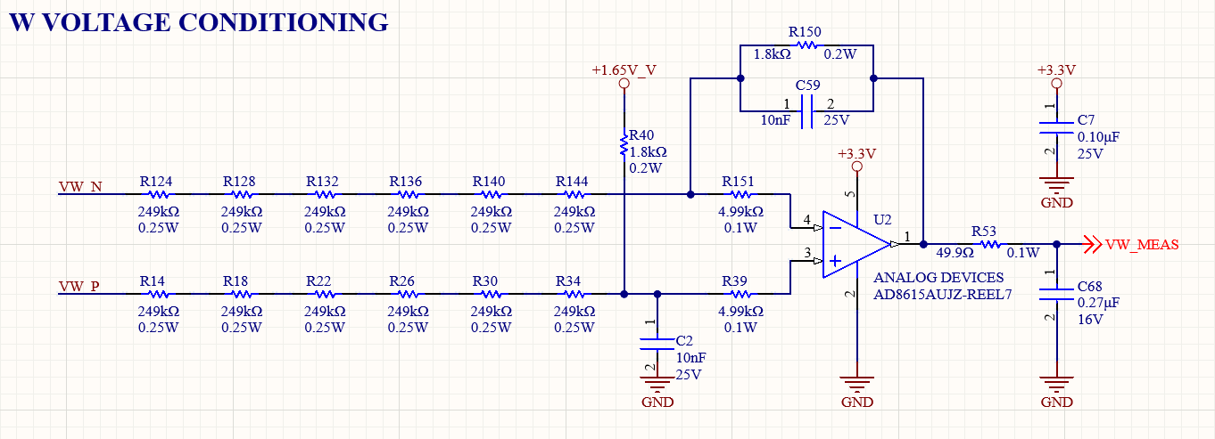
- Regarding grid voltage sensing, I noticed that this design does not use isolation but instead relies on resistors and an operational amplifier to sense the voltage. The same approach is used for inverter voltage sensing and DC bus voltage sensing. I’m wondering if this could cause any issues due to the high voltage involved. I’ve attached an image of the circuit used to sense one of the grid voltage phases.
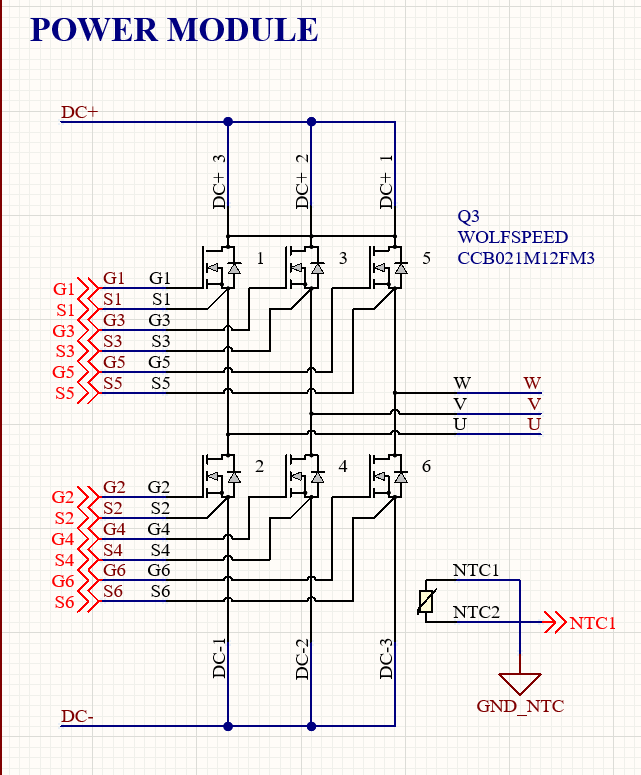
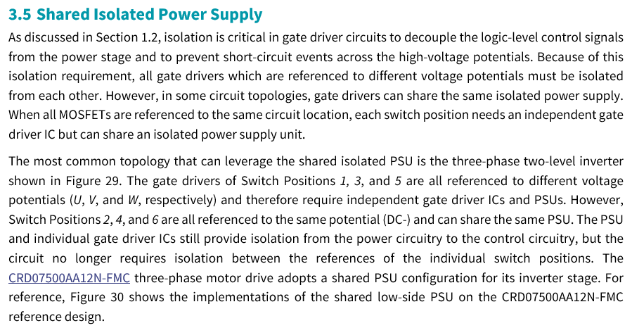
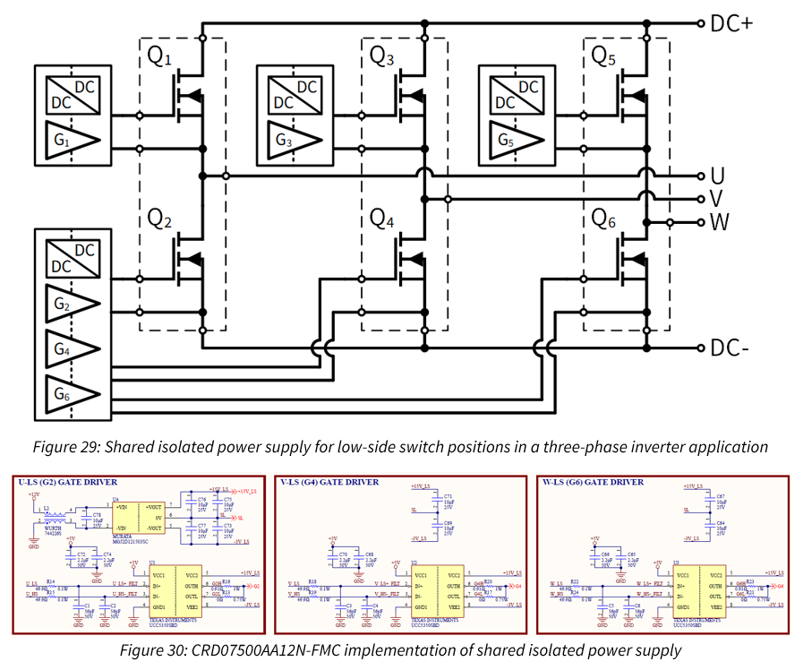
2. My second question is about the isolation between the inverter's MOSFETs. As shown in the attached image, the design uses isolated power supplies for the gate drivers of Q2, Q4, and Q6. If I were to implement this design using discrete MOSFETs instead of the module used in the reference design, could I share the same voltage zone for these three MOSFETs?
3. Finally, I noticed that the module does not use a snubber circuit. Is it unnecessary in this design? If so, could you explain why?
I would really appreciate any guidance on these points.
Thanks!
Comments
-
Thank you for your post, it has been approved and we will respond as soon as possible.
0 -
Hello EChemetal,
Thank you for your interest in this product. I addressed your questions individually below.
- The design uses differential measurements with high impedances for both the signal and reference paths. The resistor chains introduce the necessary creepage and clearance distances and prevent hazardous voltages from reaching the controller. This is a common approach adopted in these types of designs. An additional isolation barrier could be added in series with this circuit, if necessary. For example, the CRD60DD12N-GMB uses an isolated operational amplifier for isolation.
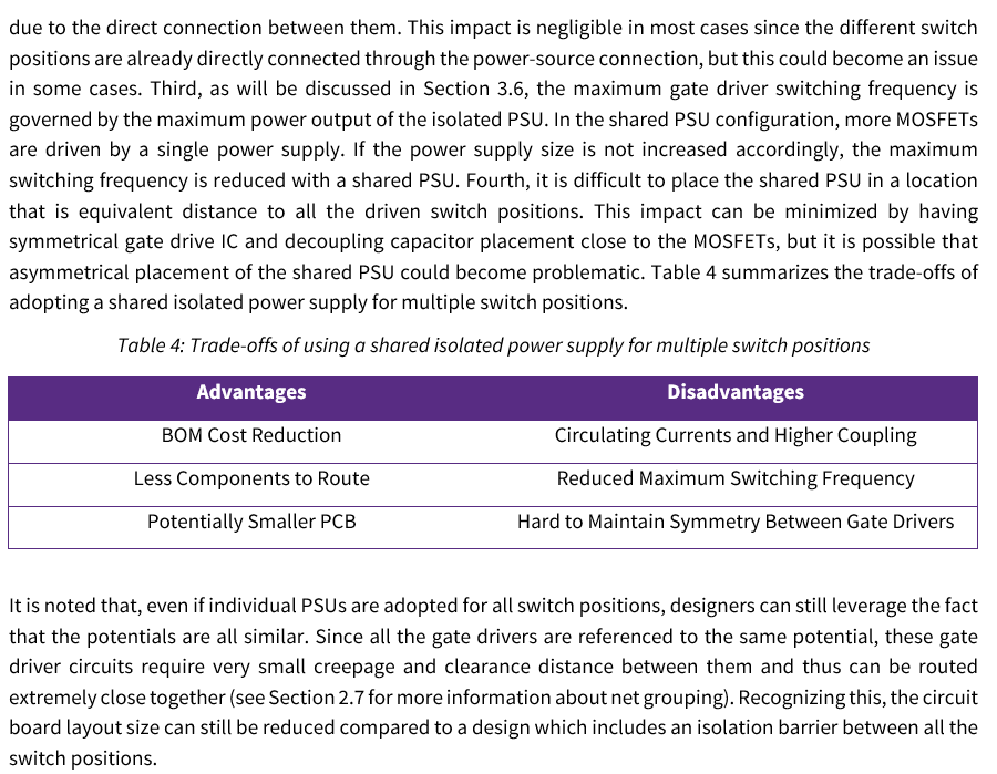
- You can share the same isolated power supply for the three indicated gate drivers (Q2, Q4, and Q6). This is not a unique feature for discrete devices. The CRD07500AA12N-FMC motor drive design features a shared isolated power supply for the low side switches. Deciding whether to adopt a single isolated power supply is dependent on the circuit routing and target switching frequency. See the below information from an in-progress Application Note for more details about these tradeoffs.
- This design uses low inductance routing (interleaved DC+ and DC- copper pours) with a high-performance power module. Minimal drain-to-source voltage overshoot is observed in this circuit, so the snubber was not necessary.
Thanks,
Chris N.
0