
SpeedFit™ Design Simulator
Simulate and evaluate the performance of SiC-based power circuits and determine the right SiC device in seconds.
Start a Simulationpremature overcurrent tripping of gate driver CGD1200HB2P-BM3

I am having some trouble with a switching power supply which uses Si Ca MOSFET switch pair CAB530M12BM3 and a gate driver CGD1200HB2P-BM3 driver driven by a CGD12HB00D transceiver.
The problem is that if I try to increase the current much beyond about 300A, the driver will trip on over current. This current is no where near the level that should cause a trip. I am looking for reliable running at 600A.
My question concerns the gate driver gate driver CGD1200HB2P-BM3. How much time is allowed after sending the gate voltage high, before the drain source voltage limit of 2.9 volts is activated?
It surely takes time for the Si Ca MOSFET to switch on and the drain source voltage to come down.
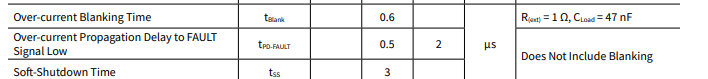
There doesn’t seem to be any mention of this time in the data sheet for the driver other than the over current blanking time of 0.5 to 2us. Is this the time that I am referring to? If so it seems very short, in our case it takes longer for the voltage to settle below the threshold.
Oscilloscope trace below shows the Drain Source voltage of the high side device while running at about 320A. the voltage is measured down from the Drain (+ve dc rail) (the scope probe is protected by 100k resistance and 5v1 zener, hence the -5v limit).
The DS voltage does falls to a bit less than a volt but seems to take about 2.5us to get below 2v.
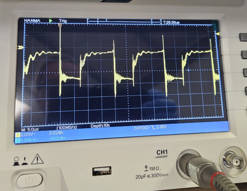
The gate drive resistors are unchanged at 1R, however the Zener diodes DB2 and DB10 have been changed from 5v1 to 3v9 to give a 1.2v increase D-S trip voltage from 2.9v to 4.1 v. This was done in an attempt (unsuccessful) to fix the over current trip problem. The trace shows some ringing as the D-S voltage comes down, is this normal?
Background info. The circuit runs as a simple buck regulator with low side device acting as flywheel diode, running at 50 kHz, the control circuit is based on a current mode control chip UC3843, the high side and low side devices are driven in anti-phase with dead times (anti overlap) of at least 100ns, these are generated in my control circuit. The whole system is driving a flash lamp in pulse mode, i.e. it is intended to flash the lamp for typically 1 to 10 ms and 1 to 100Hz but with the mark space ratio of never more than 10%. Current 100 to 600A, supply 900v across a substantial capacitor bank. The output (lamp) pulses are switched on and off using the PWM-En control, the PWM runs continuously.
I look forward receiving any guidance on this.
Ianp
Comments
-
Thank you for your post, it has been approved and we will respond as soon as possible.
0 -
Hello Ianp,
The blanking times of 0.5 µs to 2 µs is correct. This is a typical range for protecting SiC devices. Short circuit events longer than this range risk catastrophically destroying the part. There are a few things to consider for your setup.
- Power loop inductance is a critical factor in system ringing. If the circuit board layout has significant power loop inductance, that power loop noise will coupling into the overcurrent (DESAT) circuit and likely cause false overcurrent triggers. I recommend scrutinizing your power layout to ensure that you are adhering to best practices to reduce power loop inductance.
- A deadtime of 100 ns is aggressive for the CAB530M12BM3 power module. Even if you have anti-overlap protection, you still must still consider the non-instantaneous rise/fall times of the devices themselves. It is possible that you are observing DESAT challenges due to partial shoot-through conditions (both switch positions on). I recommend measuring both complementary switch positions simultaneously to see if the turn-off events are complete before the turn-on events begin.
- Are you able to attach a high bandwidth current measurement in your power loop to observe whether you have high-current dynamics actually following through your system? A Rogowski coil would likely be the easiest method to add to the circuit and has sufficient bandwidth for this measurement. With the measurement in place, you could configure the oscilloscope to trigger on a spike in the current measurement. Perhaps the DESAT circuit is actually tripping as expected due to a spurious control signal.
- Using oscilloscope probes with long ground leads can introduce artificial noise in the system. It is possible some of the ringing in your oscilloscope measurements shown are due to the oscilloscope measurement setup and not representative of the circuit dynamics.
- You can increase the blanking time of the device by increasing the size of the DESAT blanking capacitors, CB9 and CB21. This will extend the amount of time that the gate driver ignores noise after a switching event. Please note that increasing the blanking time significantly can risk damaging the device since the DESAT circuit will no longer trip in a suitable amount of time to save the device.
Some additional details about DESAT circuit implementation is discussed in Section 5.1 of PRD-09301.
Thanks,
Chris N.
0 -
Thank you Chris,
I will increase the dead times that I generate on my control PCB, 200ns? I will also measure the supply current with an Ro probe.
At point 5 you mention changing DESAT Blanking, I don't see any mention of that on my driver's data sheet or CB9 and CB21, however it seems that this is not the best thing to be doing, at least until other things are improved.
I have a raft of improvements to make to clean up signals, e.g. screening power cables in close proximity to the control pcb and as they pass through the current transducer which provides feedback to the PWM generator circuit.
Many thanks for you answer, I will report back once the work is done.
Ian
0 -
Hello ianp,
Thank you for the update. As you already indicated, improving the circuit inductances and routing signals away from high dV/dt and di/dt signals is the best place to start. Many problems can often be solved by scrutinizing signal chains and searching for signals with high unwanted coupling.
Modifying the blanking time is not something that is generally done which is why it is not included on the datasheet. It's typically only modified by advanced users wanting to evaluate edge conditions or operate the power module in unique conditions. If you are not comfortable making this change, I recommend focusing on the other changes I recommended.
If you build your circuit topology in LTspice using the Wolfspeed models (here), you can look at the expected rise/fall times at your operating conditions to estimate the minimum required deadtime. This can also be determined with the experimental measurements you have planned.
Thanks,
Chris N.
0 -
Hello ianp,
I hope that this answered your question. I will close this discussion for now but if you have a follow up question, please "Start a New Discussion" and we would be glad to support you further.
Thanks,
Chris N.
0