
SpeedFit™ Design Simulator
Simulate and evaluate the performance of SiC-based power circuits and determine the right SiC device in seconds.
Start a Simulation3rd Quadrant Operation in plecs models

I'm using the plecs models offered by Wolfspeed and I have problems understanding how the conduction losses in revers conduction mode with activated gate voltage are calculated. The devices I'm interested in are CAB650M17HM3 (combined MOSFET with diode model) and CAS310M17BM3 (individual MOSFET and diode model).
For the CAB650M17HM3 there is only one file which has conduction losses for both current directions for both cases (gate on or gate off). This is pretty straight forward. The on-state voltage curve is asymmetric, which is expected since the anti parallel diode takes over part of the current in reverse conduction (3rd quadrant) operation.
In case of the CAS310M17BM3 device, however, there is two devices now. The MOSFET alone still has an on-state voltage curve, which also reaches into 3rd quadrant. It is also asymmetric, i.e., it seems to include the effect of the body diode. However, the diode model itself also has an on-state voltage curve. This is likely the one to be used when the device is turned off, but which one is now valid when the device is turned on? The one given by the MOSFET? Or do I have to consider the parallel combination of the two elements with the current sharing calculated online by the simulator? This is relevant for me because I want to use the data from the plecs model XML files in an optimization outside of plecs.
An additional question arises from the thermal resistances. The CAB650M17HM3 datasheet only mentions a thermal resistance of the FET, which is relevant for the total losses of the device. In case of the CAS310M17BM3 , different Rth values for MOSFET and diode are listed. This suggests that diode and FET losses would have to be treated individually.
Comments
-
Thank you for your post, it has been approved and we will respond as soon as possible.
0 -
Dear Wolfspeed,
unfortunately I didn't hear back from you. Meanwhile, I identified two other aspect which are very like errors in the plecs model for the CAB600M33LM3 device:
- The datasheet curve for the Rds,on vs drain-source current don't match the table in the datasheet:
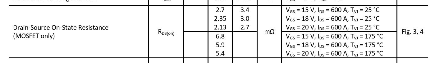
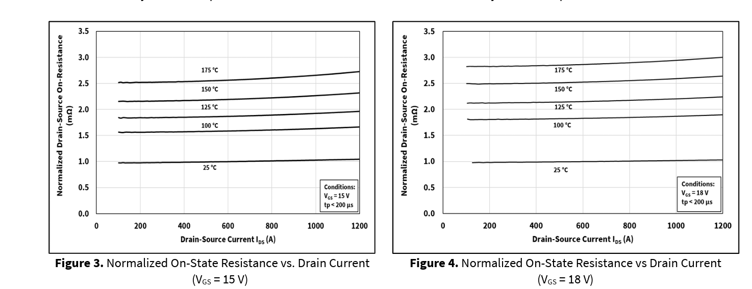
For 175 °C I don't obtain the values specified in the table for 600 A and 18 V gate voltage.
- The switching losses in the plecs model differ from the datasheet by roughly a factor of 2 for Eon and Err. For example in Fig. 21:
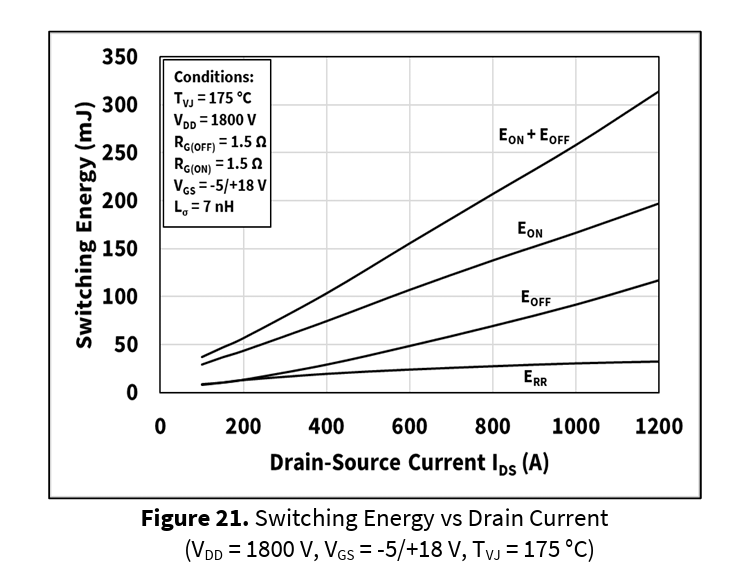
For drain a current of 600 A and 175 °C, you would expect reverse recovery, turn-on and turn-off energies of 25 mJ, 110 mJ and 50 mJ, respectively. In the plecs model, I get 54 mJ, 200 mJ and 43 mJ.
Could you comment on these?
0 -
Hi mchvltg,
First, let me address your original inquiry.
The key is that the "S" vs "B" in "CAS vs "CAB" denotes that the module has a parallel Schottky diode inside (in addition to the MOSFET devices). This means the model represents the two chips separately (which is why there are two Rth values for CAS modules, while only one is needed for a CAB module). For all modules, the MOSFET PLECS model represents all parallel MOSFET in the switch position and similarly the diode model for the CAS module reflects all parallel Schottky’s.
As you note, the MOSFET with Diode models (such as the CAB650M17HM3) have tables for both gated on and gated off conduction losses.
Looking a little deeper at the CAS module model in third quadrant conduction, because there is a parallel Schottky, the situation becomes a bit more complex due to current sharing between the two types of devices. When the MOSFET is gated off, the higher forward voltage of the body diode means that the conduction behavior will be dominated by the Schottky, and (in practice) the contribution of the body diode can be ignored. This behavior is accurately captured in PLECS because the MOSFET model is implemented as a "MOSFET" model (instead of a MOSFET with Diode" model), which means when the part is gated off, it will not conduct in the reverse direction. When the MOSFET is gated-on, however, the MOSFET resistance tends to be lower than the Schottky voltage drop, leading to the majority of the current flowing through the MOSFET. Of course, once you look across temperatures and current levels, it’s easy to find cases where the current sharing is less one sided.
The CAS model in PLECS, however, is not able to capture this nuance. We chose to compromise and set the gate-on 3rd quadrant conduction losses in the MOSFET model to the measured 3rd quadrant of the entire module (which includes both MOSFET and Schottky behavior – i.e. the model matches figure 5 of the datasheet). While this will lead to slightly more losses in the MOSFET (i.e. we are modeling that all current goes through the MOSFET while, in reality, some should be in the Schottky) and a slightly higher Tj, this approach at least achieves accurate total losses. It might seem preferable to separate the MOSFET 3rd quadrant conduction without the Schottky, but that would only work if PLECS could accurately model the current sharing between the Schottky and MOSFET. Because the electrical model in PLECS heavily simplifies the semiconductors to a resistance and forward voltage (for the diode) and has no temperature dependence, this approach is far less accurate in my experience.
I know that’s a long-winded explanation, but I assume that you might need such detail given that you are trying to use the data outside of PLECS. Let me know if you have any other questions on our implementation or module performance.
As for the CAB600M33LM3, I agree with your analysis, there are multiple issues to address in both the datasheet and model. I've checked in with the product manager and can share that there is a major update planned for that datasheet (at which point the model will be fixed also). The current model is conservative, so I'd expect any simulation results to improve once that update is released.
Thanks for your inquiries,
Blake0 -
Dear BlakeNelson,
thank you very much for your detailed explanations, these help a lot. I already assumed that there might be an additional chip involved, but I wasn't entirely sure how Fig. 5 had to be interpreted exactly (whether only the FET or the entire parallel combination was included). Thanks for clarifying.
0