
SpeedFit™ Design Simulator
Simulate and evaluate the performance of SiC-based power circuits and determine the right SiC device in seconds.
Start a SimulationHS & LS bias in CDG1700HB2P-XM3

Hello:
Can some one explain how HS_VDD and LS_VDD all are 5V in CDG1700HB2P-XM3?
Should they not be of gate drive capable voltages tied to the respective halfbridge nodes?
Furthermore, in some other App note on Gate Driver board, the bias levels developed are +25V and -5V
In the App Note in discussion here, there is nowhere any such bias voltages one can see.
One more thing: In the App Note where 25V is generated, one cannot locate how that can be applied to any TI or any other gate driver VDD pins. They are all restricted to 18V . Some, maybe to 22V.
Appreciate clarification of these issues.
-robin
Comments
-
Thank you for your post, it has been approved and we will respond as soon as possible.
0 -
Hello Robin,
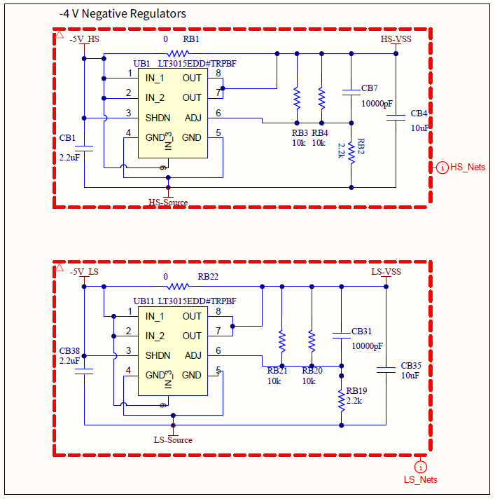
The HS_VDD and LS_VSS voltages on the CGD1700HB2P-XM3 gate driver are +15 V by default. These voltages are generated by the isolated DC/DC converters UT1 and UT6. I provided a picture from the schematic below showing where these voltages are generated. The schematics and additional design files can all be downloaded from the CGD1700HB2P-XM3 landing page for further review.
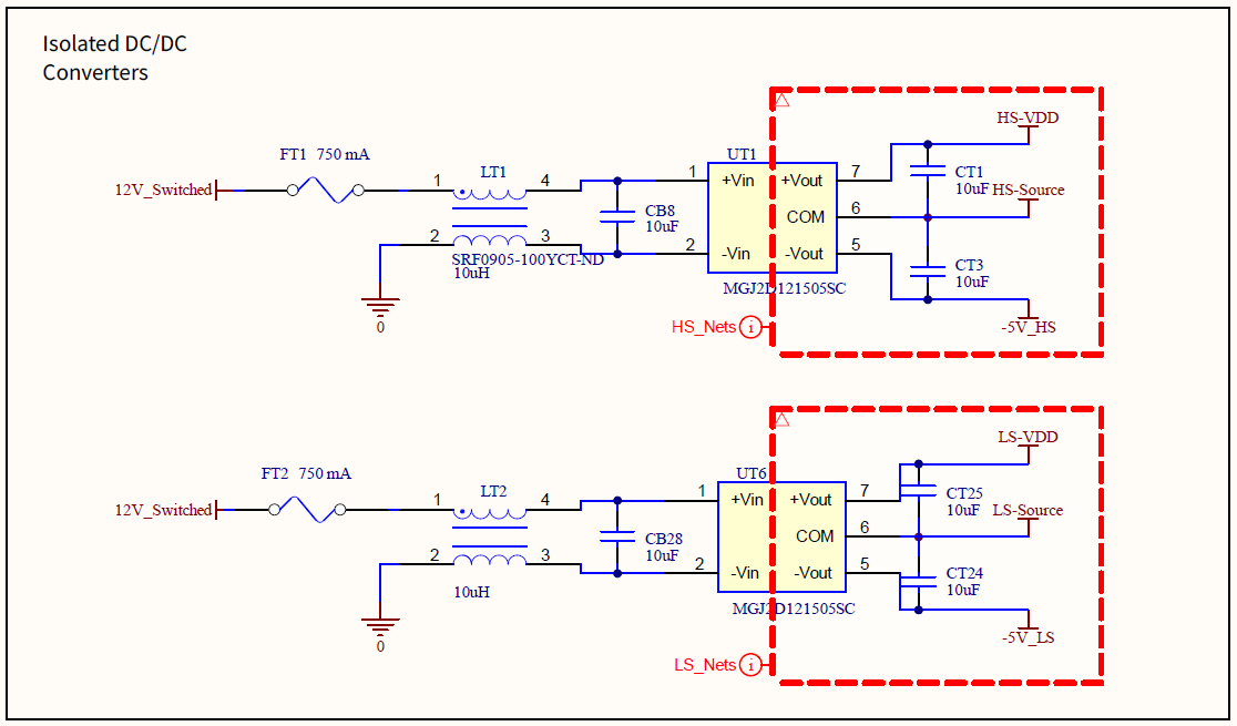
The Murata MGJ2D121505SC DC/DC converter generates split output voltages of +15 V and -5 V, with respect to the source terminal. The -5 V rail is then adjusted to -4 V using a linear regulator (shown below) to achieve the target gate driver voltages of +15 V for turn-on dynamics and -4 V for turn-off dynamics. If you require different gate driver output voltages, you can swap the isolated DC/DC converter (which is a standard footprint) for one with different output voltages and equivalent isolation rating. For example, the Murata MGJ2D121805SC generates a +18 V / -5 V output. Alternatively, if you only need to change the turn-off voltage, you can vary the negative linear regulator output.
If you have further questions, can you please mention which document you are referencing? In some of Wolfspeed gate driver designs (such as the CGD1700HB2M-UNA), two linear regulars can be added for independent precision tuning of both the turn-on (VDD) and turn-off voltages (VSS). In these cases, it can be advantageous to use an isolated DC/DC converter with a large dynamic range (such as +25 V / -5 V like you indicated) since it provides designers with a lot of flexibility to tune the required output voltages with the linear regulators. Perhaps the document that you are referencing was adopting this approach. Wolfspeed recently released the PRD-09301: Gate Driver Design for SiC Power Modules which might be a useful resource for you if you are designing your own SiC gate driver solution.
Thanks,
Chris N.
0 -
Hi, I hope that this answered your question. I will close this discussion for now but if you have a follow up question, please "Start a New Discussion" and we would be glad to support you further.
0