
SpeedFit™ Design Simulator
Simulate and evaluate the performance of SiC-based power circuits and determine the right SiC device in seconds.
Start a SimulationContinued overcurrent tripping of gate driver CGD1200HB2P-BM3 driving CAB530M12BM3 via CGD12HB00D t

I am still having trouble with premature overcurrent tripping> following my post and your answers from Sept 2025, I have increased the dead time from the " aggressive 100ns" to 1.1us I have also run for a short time with the LS device disabled, relying on its diode for flywheel duty. It still trips, so it definitely is not shoot through.
Background info. The circuit runs as a simple buck regulator with low side device acting as flywheel diode, now running at 30 kHz. the inductor is 100uH and air cored, just a coil of 35mm2 cable. The whole system is driving a flash lamp in pulse mode, i.e. it is intended to flash the lamp for typically 1 to 10 ms and 1 to 100Hz but with the mark space ratio of never more than 10%. Current 100 to 600A, supply 900v across a substantial capacitor bank.
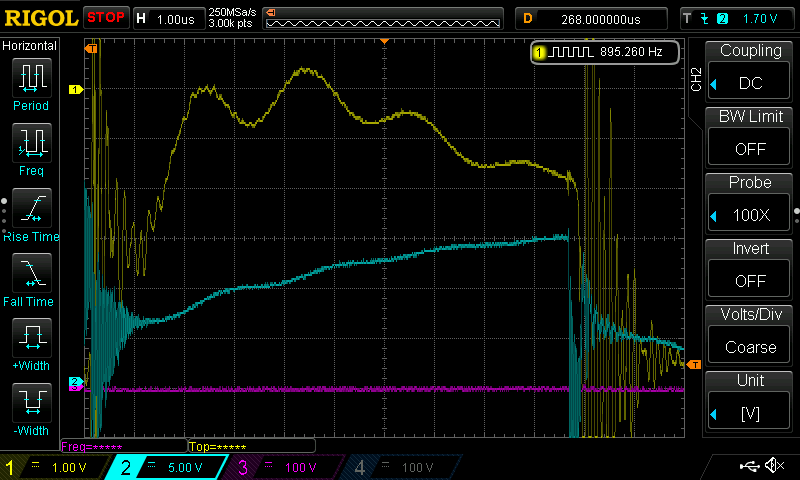
I have attempted to measure the HS Vds again at the same time as the HS gate pulse. this was precarious! with the scope battery powered and floated to dc link voltage with voltage clamp to protect the standard scope probe used for the Vds and a differential probe for the gate. Not ideal as the diff probe leads are long separate wires. however I judged the Vds should be reasonably accurate and the timing from the beginning of the gate pulse to Vds coming below 2.9v is visible.
The yellow trace in volts, clamped at 5.1v, measuring down from HS drain, Blue is the gate voltage rising.at 5v/div. Gate resistors on the CGD1200HB2P-BM3 are all 1R. The Vds seems to come below 2.9v after about 1.6us even though these conditions did not trip. Obviously the noise and some measurement in accuracy muddies the water a bit but the general theme seems that the Vds stays around 3v and then starts to reduce after about 1.5us.
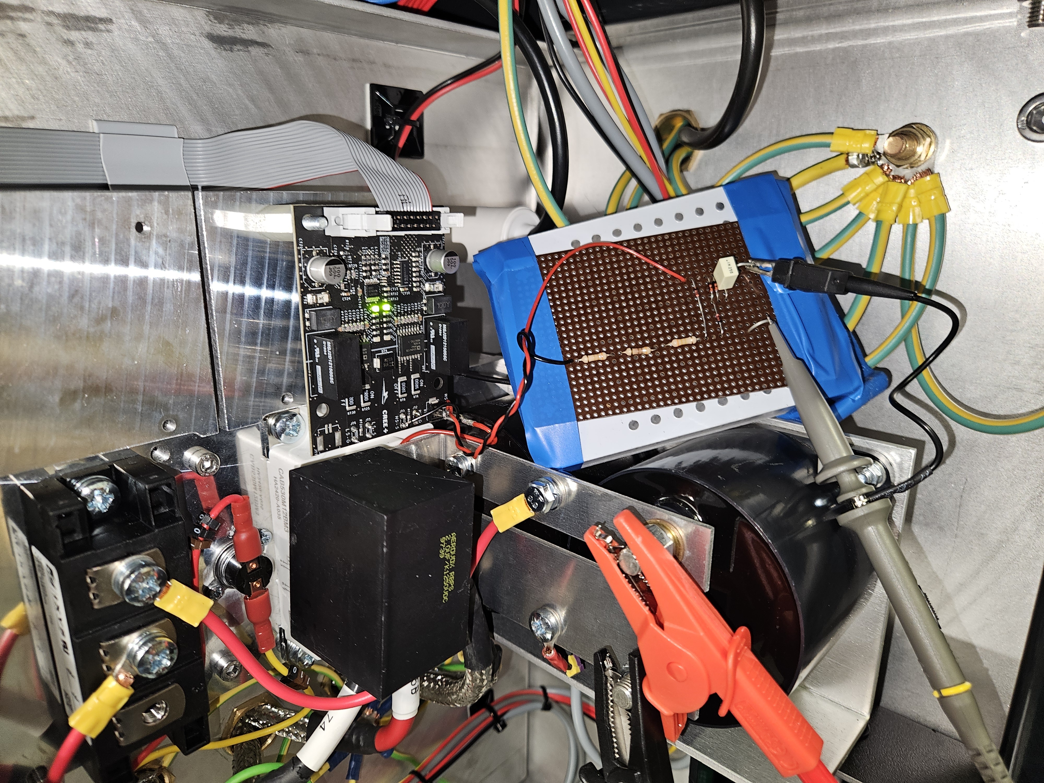
You mentioned in your answers to my previous post, that power loop inductance is a critical factor in system ringing. At these power levels I am not using a PCB, there are cables coming from the 900v capacitor bank, these run as a parallel pair as far as is practical but the capacitors are big and some inductance is unavoidable. I have a lot of capacitance across bus bars to the Power Mosfet pair, 100uF, a 50uf coupled as closely as possible with a further 2uF directly across the MOSFET terminals. I have looked at voltage here and the overshoot at when the HS switches off is very minimal bump. I have a Rowgowski probe but I cannot physically put it around the HS drain connection because the metalwork bus bars are so closely coupled, I imagine the high frequency ringing is coming from the local capacitors rather then the bigger power loop.
Photo of the layout below, the clamp for measuring the Vds is temporarily attached.
I am temped to increase the over current trip blanking time by increasing the value of value of CB9 and CB21 of the driver, currently 56pF, I have ordered some 100pF 0603 components in case. I note that you don't recommend this but question will the device really be damaged by an over current lasting say 2us?
Thank you in anticipation for any guidance, I can supply more detail if needed.
Ian
Comments
-
Thank you for your post, it has been approved and we will respond as soon as possible.
0 -
Hi Ian,
I recommend changing the values of DB2 and DB10 to a 0 Ω 1206 resistor to push the overcurrent trip level to its highest setpoint. During a short circuit event, this will still allow the driver to detect a fault very quickly.
If you're still experiencing tripping, you can try to increase the blanking time with the capacitors you mentioned, but it's typically best to keep these values as small as possible. Yes, the device can be damaged with a short circuit even lasting just 2 µs. In fact, ~2 µs is commonly the short circuit withstand time of a SiC MOSFET; we recommend targeting a 1 µs detection and extinction of a short circuit fault.
Best Regards,
Austin C.
0 -
Hello Austin
Thank you for the answers, I have replaced the zeners DB2 and DB10 as you suggest, this has enabled me to go higher in current but I am concerned that I need to do it. The gate driver and MOSFET pair are designed to work together. From my oscilloscope image it looks as though the CAB530M12BM3 is just not being turned fast enough despite using the CGD1200HB2P-BM3 driver with 1R gate resistors. My dc link is as stable as I can make it with low inductance polypropylene capacitors 100uF, 50uF and 2uF connected as close as possible to the Mosfet terminals, lowest value directly so.
However I am now wondering if I need to add some snubbers to the mid terminal that goes to my inductor and load, as there is alot of ringing on that terminal. Could this be disrupting the turn on? Do you have any guidance on snubber design for use with these semiconductor switches.
Best regards
Ian
0