
SpeedFit™ Design Simulator
Simulate and evaluate the performance of SiC-based power circuits and determine the right SiC device in seconds.
Start a SimulationCRD25DA12N-FMC Voltage, Current, and Resolver Reference Rails 5V Input

Hello,
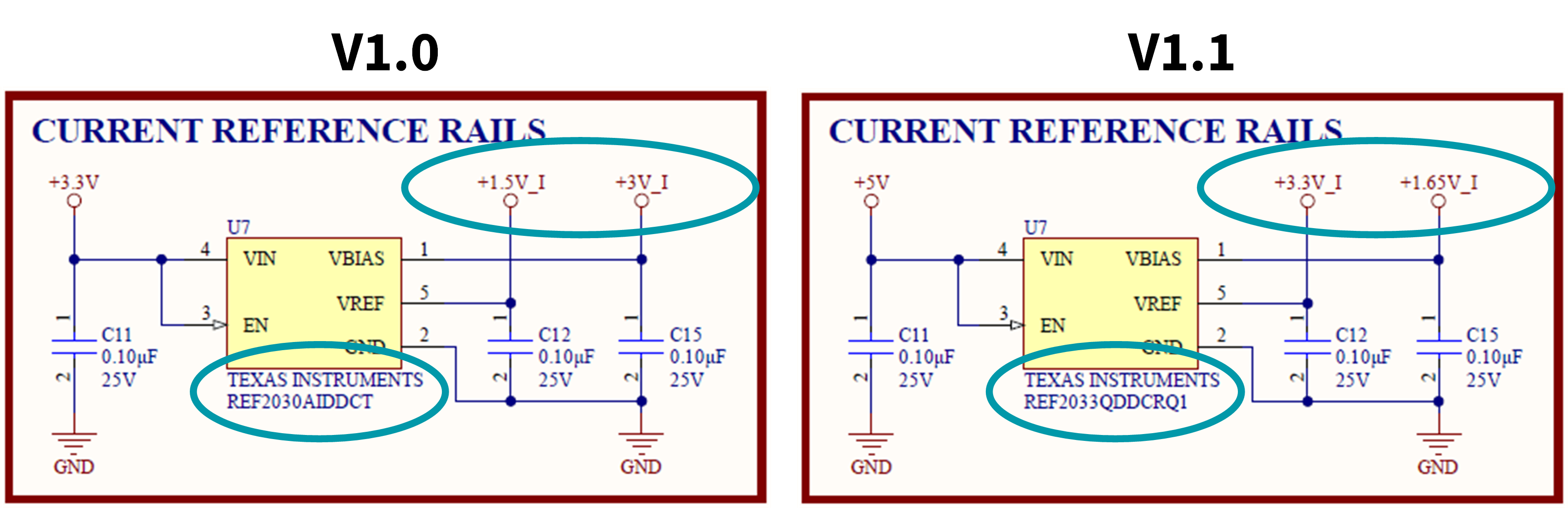
I've been testing the Current Sensing circuits for Phases U, V, and W and noticed that the ADC voltage (I_MEAS) is incorrectly at 0.761V instead of 1.65V (3.3Vref/2) when the input phase current is 0A. This is throwing off the ADC read on my simulation, resulting in incorrect current sense values. When measuring voltage at the Current Reference Rail (U7), I noticed where there should be a 5V input at pins 3 and 4, there is actually a 3.3V input, decreasing Vref to 3V and Vbias to 1.5V. Going even further, the schematic and board design shows that R154 should be pulled up to the +3.3V_I rail, however, a continuity test shows that it is actually being pulled up to the +1.65V_I rail (actually 1.5V with incorrect input voltage to U7).
The same voltage issue is present at U38 and U48. I have module V1.0, but I checked the schematics for the later versions and there is no change to these nets.
Comments
-
Thank you for your post, it has been approved and we will respond as soon as possible.
0 -
Hello AOgorzaly,
This is a known error in the V1.0 hardware that was quickly addressed in V1.1 and onward. The VBIAS and VREF pins were incorrectly flipped. VBIAS should be connected to the +1.5V_X rail and VREF should be connected to the +3V_X rail. I provided a picture below comparing the current reference rail connections in the V1.0 hardware vs the V1.1 hardware; the voltage rail connections are flipped. We also took the opportunity to change from +1.5V/+3.0V rails to +1.65V/+3.3V rails by switching from the Texas Instruments REF2030 to the Texas Instruments REF2033. This change enables the design to take advantage of the full 0V to 3.3V dynamic range of the the analog-to-digital converters (ADC) on the Texas Instruments TMDSCNCD280039C controller.
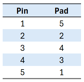
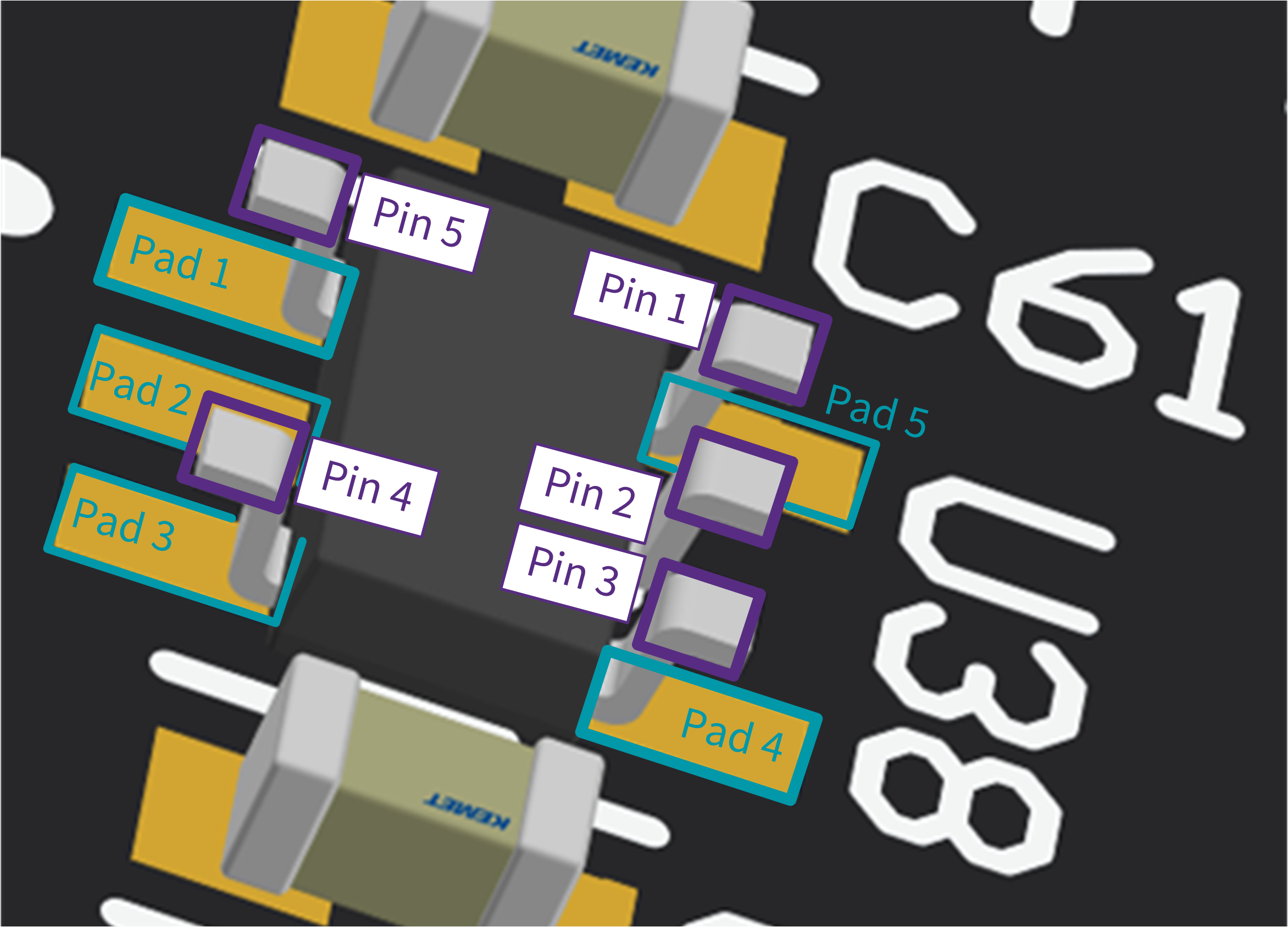
The easiest way to fix this issue is to desolder the voltage reference integrated circuits (U7, U38, and U39 on V1.0 hardware), flip the chips upside down, and solder it following the connections listed in the table below. Each of these pins will solder directly down except for Pin 2 / Pad 2 which will require a small jumper wire. This change will flip the +1.5V and +3.0V connections to enable the circuit to function properly.
Thanks,
Chris N.
0 -
Hello AOgorzaly,
I hope that this answered your question. I will close this discussion for now but if you have a follow up question, please "Start a New Discussion" and we would be glad to support you further.
Thanks,
Chris N.
0