SpeedFit™ Design Simulator
Simulate and evaluate the performance of SiC-based power circuits and determine the right SiC device in seconds.
Start a SimulationDefinition of E_RR for SiC Module

Hello Wolfspeed team,
I am working with the CAB004M12GM4 SiC half-bridge module.
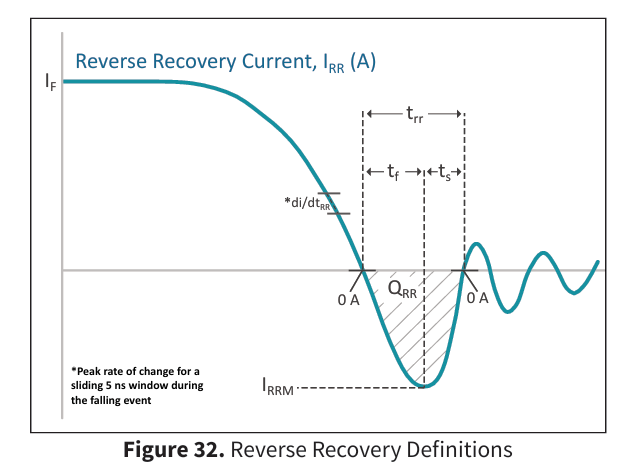
The datasheet gives definitions and values for body diode reverse recovery time t_rr and reverse recovery charge Q_rr, but there is no formal definition provided for reverse recovery energy E_RR.
Could you please share your official definition of E_RR that is used for the datasheet characterization from double pulse testing? Specifically:
- Exact start point of the integration
- Exact end point of this integration
- Whether linear extrapolation is used, or whether parasitic ringing after recovery is excluded from the integration
We need this integration window information to align our double pulse measurement results with the E_RR values listed on the datasheet.
Thank you.
Comments
-
Thank you for your post, it has been approved and we will respond as soon as possible.
0 -
Hi Pete,
Reverse recovery energy uses the same integration bounds as QRR, but Irr*Vrr is integrated instead of Irr. The typical integration bound used is described in the datasheet, with integration bounds from 0/0. However, sometimes this integration method fails due to offsets or soft diode recovery behavior, in which case an alternative extrapolation method is used. Take a look at the attached APEC presentation, specifically slide 7, that describes this method. The overall change in calculated charge/energy is small, but it is more consistent at finding the proper final integration bound.
Thanks,
Brian
 0
-
Hi,
0 -
Hi Brian,
Thank you so much for sharing the official Err definition.
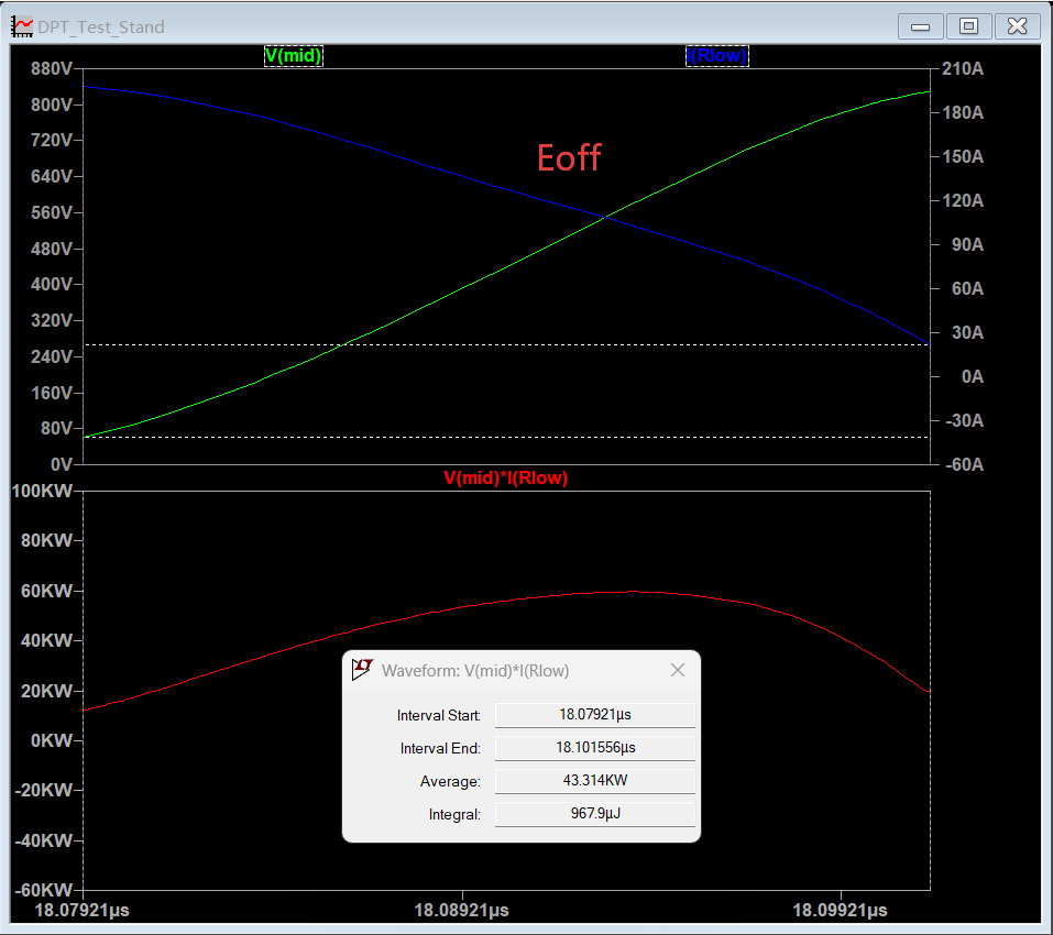
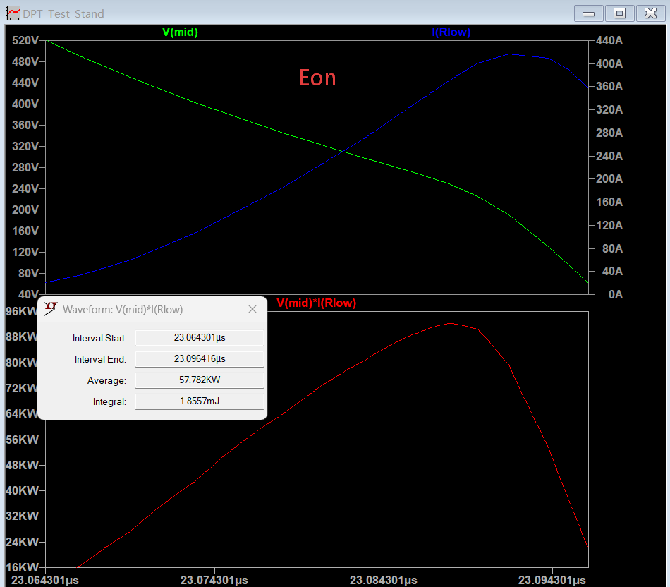
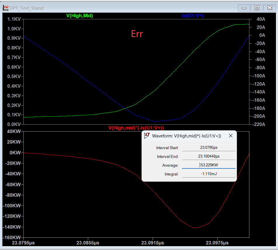
I simulated the official CAB004M12GM4 model in LTspice under datasheet conditions: Vtj=25℃, Vbus=600V, ChargePulseTime=17µs(Is=200A), Vgs=-4V/15V, Lbus=11nH, Rg=0Ω.
My results: Err=1.5mJ (datasheet 1.3mJ), Eon=1.6mJ (datasheet 2.2mJ), Eoff=1.2mJ (datasheet 1.0mJ).
Unfortunately, I cannot add screenshots or attachments here because of network issues.
There are some deviations from the datasheet typical values. It would be very helpful if you could give some suggestions on what might cause this difference.
0 -
Hi Pete,
First, you should add ~0.7Ohm Rgon and 0.3Ohm Rgoff to include the influence of the gate driver IC resistance. That may help tighten up Err/Eon.
I loaded up the model & data used to generate the datasheet and ran my comparison tool. The same calculations are performed on the empirical and simulated data. I get:
Eoff: 1.13mJ, Eon: 2.26mJ, Err: 1.36 mJ
Here are the waveforms (blue empirical, orange simulation):
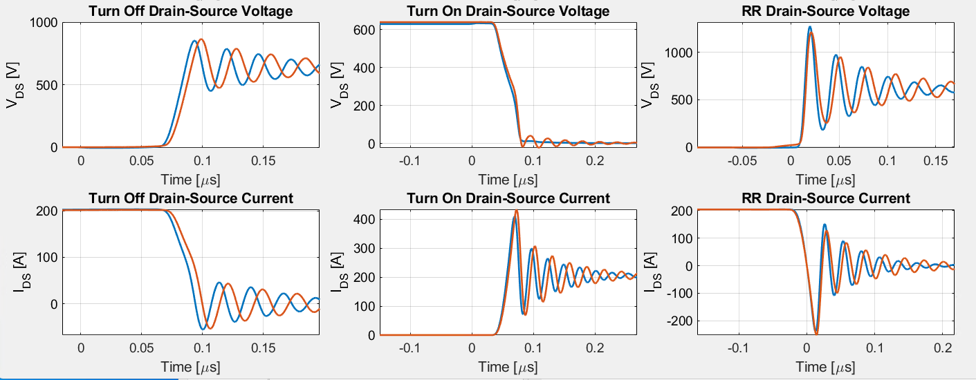
How are you calculating SW losses with the simulation?
Let me know your new energy values with the adjusted Rg.
Thanks,
Brian
0 -
Hi Brian,
Thanks a lot for your detailed reply and waveforms! I set up the simulation as you suggested, and my results are Eoff=0.98 mJ, Eon=1.86 mJ, Err=1.18 mJ, which differ from your reference simulation.
Here are my detailed settings for your review:
- Simulation conditions:Vbus=600V, Is=200A (L=50µH, ChargePulseTime=17µs), Vgs=15V/-4V,Rg=0Ω, RgIcon=0.7Ω, RgIcoff=0.3Ω, Lh=13nH, LI=10nH, Lbus=11nH
- Integration signals: Eon(low-side) & Eoff(low-side): V(mid) * Ix(u1:V-) Err(high-side body diode): V(high,VK1) * Ix(u1:V+)
- Integration windows:Eon: 10% Is → 10% Vds (threshold definition from datasheet) Eoff: 10% Vds → 10% Is (threshold definition from datasheet) Err: IF zero crossing → Ir zero crossing (following the definition you provided before)
I would appreciate it if you could advise what causes this mismatch.
Thanks
pete
0 -
Hi Pete,
At this point, it's probably easiest if you share a .zip that contains your .asc, .asy, and .cir files so I can run your simulation.
Thanks,
Brian
0 -
Hi Brian,
Thank you very much for your suggestion. I have tried many times, but I am unfortunately unable to upload any zip files or attachments on this forum due to network restrictions.
Alternatively, would it be possible for you to share your LTspice simulation zip package including the .asc, .asy and .cir files that you used for your reference test? I can run your simulation file locally on my PC. Direct comparison with your setup will help me quickly locate the source of the mismatch.
Please let me know if this is feasible for you.
Best regards,Pete
0 -
0
-
Hi Brian,
A gentle follow-up regarding the LTspice simulation file I uploaded earlier for CAB004M12GM4.
Looking forward to your feedback on the Eon/Eoff/Err discrepancy.
Thanks a lot
0 -
Hi Pete,
I looked into this further, and these values you simulated (Eoff=0.98 mJ, Eon=1.86 mJ, Err=1.18 mJ) are fine. I was looking at the raw data, which had Vbus = 633V and Iload = 205A, which skewed the results upwards. The datasheet values will be for a true (600V, 200A) condition.
This is reasonable accuracy for a SPICE model. The model is tuned to match dvdt, didt, Eoff, Eon, Err, across Rg/Iload/Vbus/temperature, so it's quite difficult to make a model that has every characteristic accurate at every condition. If you need higher accuracy at a particular data point, you can adjust the circuit/device model a bit to match.
Example: If we change RcIcOn to 0.8Ohm, then right-click the module symbol and add 'tm1=2' to the SpiceLine, we get Eoff = 0.99mJ, Eon=2.2mJ, and Err=1.3mJ.
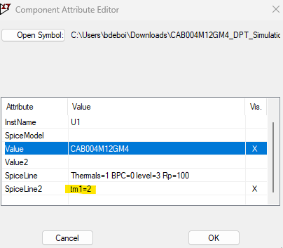
To make your life easier, you can paste this into your LTspice simulation in order to measure Eoff/Eon/Err automatically. Just press ctrl+L after running a sim to open the log & scroll down. If you run .step commands, you will also be able to plot these quantities by right-clicking in the log window and clicking "plot .meas'd step data".
- ==========================================================
- KNOWN VALUES
- ==========================================================
.meas TRAN VMAX PARAM='Vbus'
.meas TRAN IMAX PARAM='(Vbus/L)*ChargePulseTime'
.meas TRAN V10 PARAM='0.1VMAX'
.meas TRAN V90 PARAM='0.9VMAX'.meas TRAN I10 PARAM='0.1IMAX'
.meas TRAN I90 PARAM='0.9IMAX'- ==========================================================
- TURN-OFF
- Search only after first pulse edge
- ==========================================================
.meas TRAN TOFF_V10 WHEN V(mid,VK2)=V10 RISE=1 TD={ChargePulseTime}
.meas TRAN TOFF_I90 WHEN I(Rlow)=I90 FALL=1 TD={ChargePulseTime}.meas TRAN TOFF_START PARAM='min(TOFF_V10,TOFF_I90)'
.meas TRAN TOFF_V90 WHEN V(mid,VK2)=V90 RISE=1 TD={ChargePulseTime}
.meas TRAN TOFF_I10 WHEN I(Rlow)=I10 FALL=1 TD={ChargePulseTime}.meas TRAN TOFF_STOP PARAM='max(TOFF_V90,TOFF_I10)'
- ==========================================================
- TURN-ON
- Search only after second pulse begins
- ==========================================================
.meas TRAN TON_V90 WHEN V(mid,VK2)=V90 FALL=1 TD={ChargePulseTime+OffPulseTime}
.meas TRAN TON_I10 WHEN I(Rlow)=I10 RISE=1 TD={ChargePulseTime+OffPulseTime}.meas TRAN TON_START PARAM='min(TON_V90,TON_I10)'
.meas TRAN TON_V10 WHEN V(mid,VK2)=V10 FALL=1 TD={ChargePulseTime+OffPulseTime}
.meas TRAN TON_I90 WHEN I(Rlow)=I90 RISE=1 TD={ChargePulseTime+OffPulseTime}.meas TRAN TON_STOP PARAM='max(TON_V10,TON_I90)'
- ==========================================================
- REVERSE RECOVERY ENERGY (ERR)
- ==========================================================
.meas TRAN ERR_START WHEN -Ix(U1:V+)=0 RISE=1 TD={ChargePulseTime+OffPulseTime}
.meas TRAN ERR_STOP WHEN -Ix(U1:V+)=0 FALL=1 TD={ChargePulseTime+OffPulseTime}.meas TRAN EOFF INTEG '1000*abs(V(mid,VK2)I(Rlow))' FROM=TOFF_START TO=TOFF_STOP
.meas TRAN EON INTEG '1000abs(V(mid,VK2)I(Rlow))' FROM=TON_START TO=TON_STOP
.meas TRAN ERR INTEG '-1000abs(V(High,VK1)*Ix(U1:V+))' FROM=ERR_START TO=ERR_STOP0