
SpeedFit™ Design Simulator
Simulate and evaluate the performance of SiC-based power circuits and determine the right SiC device in seconds.
Start a SimulationCRD-30DD12N-K reference design : reference layer stackup of the main PCB

Hello,
With respect to the reference design of CRD-30DD12N-K, we are going to build the main board by using the PCB design file of MAIN-0816A.brd.
Meanwhile, by employing the Allegro ECAD software package, I have tried to generate the Gerber data from the PCB design file of MAIN-0816A.brd.
After completing the Gerber data generation, I have found out the reference layer stackup of the main PCB which is shown below as a captured image.
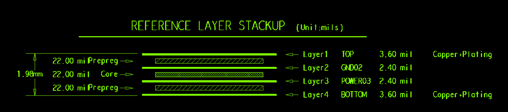
However it seems that the layer thicknesses for Layer 1 ~ 4 are not the standard thickness.
The standard copper thickness for 1oz, 2oz and 3oz copper layer is around 1.37mil, 2.74mil and 4.11mil, respectively.
Would you please review this issue?
I need to make this issue clear before I send the gerber data to the PCB house.
Thank you for your consideration.
With regards,
GKIM