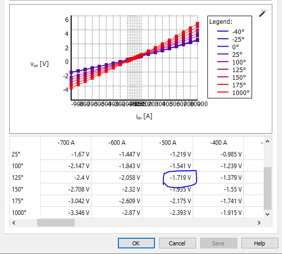
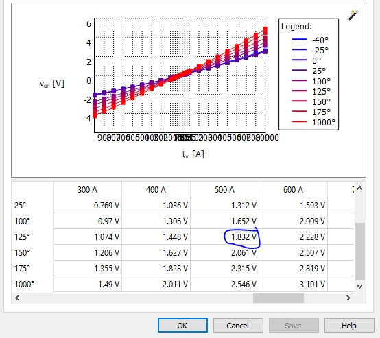
CAB450M12XM3 MOSFET I-V characteristics are different for different drain current directions.
Hi Wolfspeed team,
I would like to know why the drain-source voltage drop is different when the drain current is positive to when it is negative.
For example, at 125 degrees, the drain-source voltage drop for a drain current of 500A is 1.832V and the drop when the current is -500A is -1.719V.
Is the on-state resistance of the MOSFET lower when the drain current is negative?
Comments
-
Hello, thank you for your message. A member of our technical team is looking into your questions and we will respond shortly.
0 -
Hi Prathik,
First, it seems like you understand this, but let me make clear that the PLECS conduction model uses the datasheet data for the output characteristics (Fig. 1) and third quadrant, Vgs = 15V (Fig. 5). The specifics comparison you made would not be true for the body diode mode (CAB450M12XM3_bodydiode.xml) which is 4.362 V at 500 A, 125 °C. Put another way, the PLECS model you are looking at is designed around synchronous switching, with a fully gated on third quadrant.
Next, I will point out that the PLECS model matches the CAB450M12XM3 datasheet, which also shows that the third quadrant at 15V generally has a lower voltage drop than the forward characteristics.
Finally, while this might at first seem counter intuitive, there is a physical explanation. This paper provides an indepth explanation and is freely availed: https://www.researchgate.net/publication/318801749_Comparison_of_SiC_Voltage_Source_Inverters_Using_Synchronous_Rectification_and_Freewheeling_Diode. We are not affiliated with the authors but it would provide a deeper dive into the topic if you are interested (specifically in section II). If you look at figures 1 and 2 in the paper, you can see that in addition to the channel (which should have roughly the same resistance in both modes) there is the PN diode path, which is in parallel with the channel for third quadrant conduction. Figure 3 demonstrates nicely that the additional path provided by the diode decreases the voltage drop. In short, at low current the channel dominates as it has much lower resistance, but at higher current the diode tends to conduct most of the current. The point you selected on the curve is high enough the the body diode has a non-negligible contribution, but not high enough for it to dominate the current path. So a slight decrease in effective resistance when compared to forward seems exactly in line with physical expectations.
Let me know if that addresses your question or if you have any other questions. Thanks,
Blake
0 -
Hi Blake,
Thank you very much for your response. This is what I was looking for.
Regarding your point about the antiparallel diode's contribution to the conduction of a negative (or third quadrant) drain current, it seems to me that, even at 500A, the antiparallel diode couldn't contribute to the conduction of current in the third quadrant.
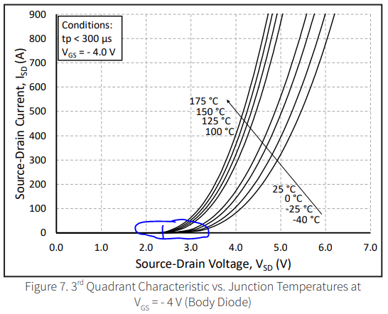
The reason why I think so is because the diode cut-in voltage is over 2V at 125C, according to the I-V curve of the diode.
From the datasheet, the max on resistance of the MOSFET is 3.7mohm (the junction temp in simulation is around 130C, so Rds(on) wouldn't be 4.6mohm), so a drain current of -500A would result in a drop of 1.87V (worst-case). This seems insufficient to forward bias the body-diode.
This is why I didn't expect the magnitude of the drain-source voltage drop to be different in the first and third quadrant.
If my understanding of this is not quite right, please let me know.
Regards,
Prathik
0 -
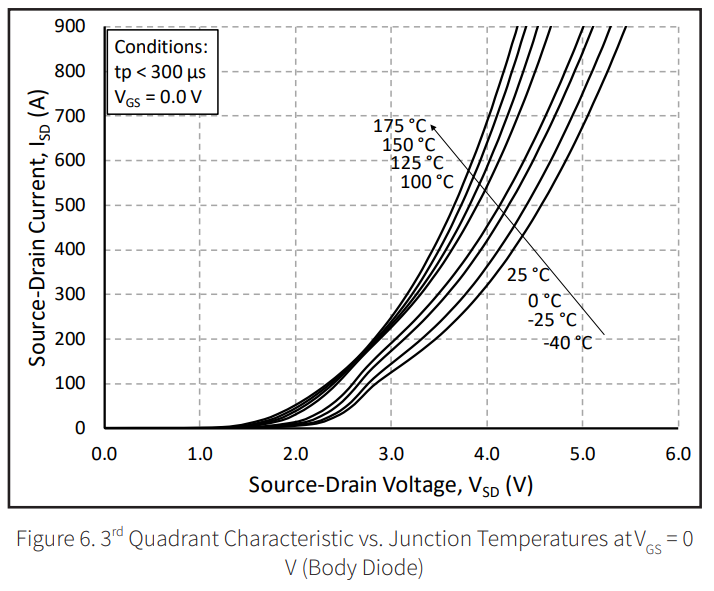
I think that is a fair point, but there is one additional bit of nuance. Basically the forward voltage of the MOSFET's body diode is also affected by the gate voltage. If we compare Figure 7 of the datasheet (which you shared) to Figure 6 (or body diode at Vgs = 0 V):
We see a dramatic increase in the current at a given voltage. Suppose for a moment, we assume that the channel resistance is equal in forward and reverse conduction for a given Vgs, then the PN junction must be changing behavior (as the channel resistance at Vgs=0 is still extremely high, since we are below threshold). If we don't assume that the channel is equal in forward and reverse, then circling back to your original question, it would be unsurprising to see a tenth of a volt difference at 500 A.
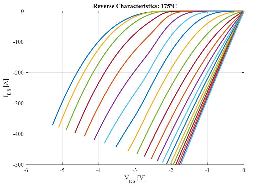
While that may already be convincing, I have a plot that I think better demonstrates my point. Here is a plot of reverse conduction for the CAB450M12XM3, with Vgs swept between -5 V and 15 V with 1 V steps:
As an aside, this data may not perfectly match the datasheet due to device to device variance.
The left two lines are Vgs = -5 V and Vgs = -4 V. The channel will not conduct any meaningful current with such low Vgs, and yet we see an increase in current with increasing Vgs (which reflects a lower threshold voltage). We can easily see that forward voltage of the body diode is highly dependent on the applied gate voltage (at least for low gate voltages). When Vgs is above threshold, it is probably impossible to differentiate between current conducted through the channel and current conducted through the PN junction. While I can't guarantee that this trend of decreasing forward voltage would continue beyond threshold voltage (device physics is not my area of expertise), I think it is clear that the voltage drop of the body diode should be much lower at Vgs = 15 V than Vgs = -4 V.
In short, my intuition is that we could assume the channel is equal resistance in forward and reverse conduction, and use the difference in the data to estimate the contribution of the body diode at Vgs = 15 V.
Happy to continue the discussion if you have further thoughts on the matter.
Blake
0 -
I think this answers my question. Thanks, Blake!.
0

