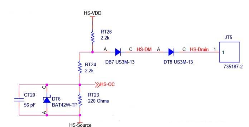
CGD1700HB2M-UNA fault signal
Dear Mr./Ms
I have bought a full set of KIT-CRD-CIL12N-FMC, including the gate drivers and transceivers. But I'm struggling to get it work. There is already some issue at initial evaluation. I hope you could help me on it.
The first one is CGD1700HB2M-UNA always generate a fault signal, right at the time the PWM is on. At the condition that no SiC is connected. means that the gate and source output are open. Nevertheless the fault signal can only be generated by over current protection on the driver.
As I looked through the schematics, the oc protection is using the desaturation circuit.
The first question, how it is working when JT5 is actually open.... The schematics told me that the only connection between gate driver and EVM board KIT-CRD-CIL12N-FMC, are the gate and source, that's it. So how the protection works?
So JT5, even it is writing as HS-Drain, but I didn't saw any connection to drain.
The second question, why HS-OC is giving me a transient rise, which exceed 0.7 V and trigger the fault protection, when I'm literally open JT5, leaves the Gate and source output open. How the PWM signal (not switching anything )is affecting the over current protection.
Could you please help?
Thank you very much!
Comments
-
Hello, thank you for your message. A member of our technical team is looking into your questions and we will respond shortly.
0 -
Hello wybcityu,
You'll need to ensure that the overcurrent protection connections are properly made; otherwise, the gate driver will immediately trip an overcurrent fault and stop switching. You cannot leave the overcurrent spade connectors open or floating on the gate driver board.
The gate driver's low-side spade connector, JT4, must be connected to the low-side drain (the midpoint) on the EVM board to enable overcurrent protection. The high-side has the same requirement; the gate driver's spade connector, JT5, must be connected to the high-side drain (V+) on the EVM board. This will prevent the LS & HS overcurrent circuits from immediately charging up and triggering a fault condition.
Best Regards,
Austin C.
0 -
Thanks you Austin, this ist clear to me.
0 -
0


