Some questions about datasheet
1. The VDSmax in the datasheet of CAB450M12XM3 limits the voltage between terminals G and S. However, in fact, SiC MOSFET will produce obvious voltage overshoot during the turn-off transient, such as 100V. If VGSmax=1200V is the limit of VDS, does it consider this 100V? Does it mean that a SiC MOSFET in CAB450M12XM3 can only work at 1100V drain-source voltage vds? Or is 1200V actually a limitation on vds?
2. Is VGS (th) the voltage between the internal pins g and s of SiC MOSFET? Because of the existence of driving resistance, vgs and VGS are quite different. According to the simulation, when VGS reaches 7 or 8 V, MOSFET starts to conduct, but the 2.5V given in the data table should correspond to Vgs?
2. In the datasheet of CAB450M12XM3, the drain current can reach 450A, but the maximum current of the body diode can reach 225A,as shown in the figure below.
If the body diode is used as the freewheeling diode of SiC MOSFET, it is easy to cause accidents. So is it necessary to parallel an SBD in practical application?
Comments
-
Hello, thank you for your message. A member of our technical team is looking into your questions and we will respond shortly.
0 -
Hi baiyujing,
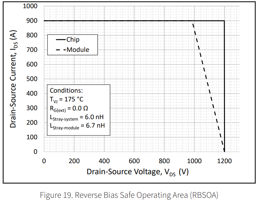
1. The drain-to-source voltage rating of the SiC MOSFET module includes any transients. So the typical maximum DC bus voltage that users of a 1200 V rated module would implement in a system is ~900 V. You need to leave room for the voltage overshoot that occurs when the devices interrupt the current in the power loop (during MOSFET or diode turn-off). The voltage overshoot that occurs is directly related to the parasitic inductance of the system, and the switching speed (di/dt), which is set by the external gate resistance. Please refer to the RBSOA plot (Figure 19) in the datasheet to see the maximum bus voltage (x-axis) that can be utilized for a certain switching speed (RG) and parasitic system inductance (Lstray).
2. The threshold voltage (VTH) is the voltage at which the channel starts to conduct a very small amount of current, which is outlined in the test conditions for VTH in the datasheet. The 7 V - 8 V range in your simulation may be where the Miller plateau occurs and is where the drain-to-source voltage transitions.
3. It's acceptable to freewheel through the body diode for the brief (typically <1µs) period during deadtime. You should not exceed 225 A continuous current during the freewheeling period. The module should be turned on (+15 V) to operate in the reverse direction (3rd quadrant) through the MOSFET channel rather than conducting through the body diode. See Figure 5 - 7 in the datasheet for the 3rd quadrant plots at different VGS.
Best Regards,
Austin C.
0 -
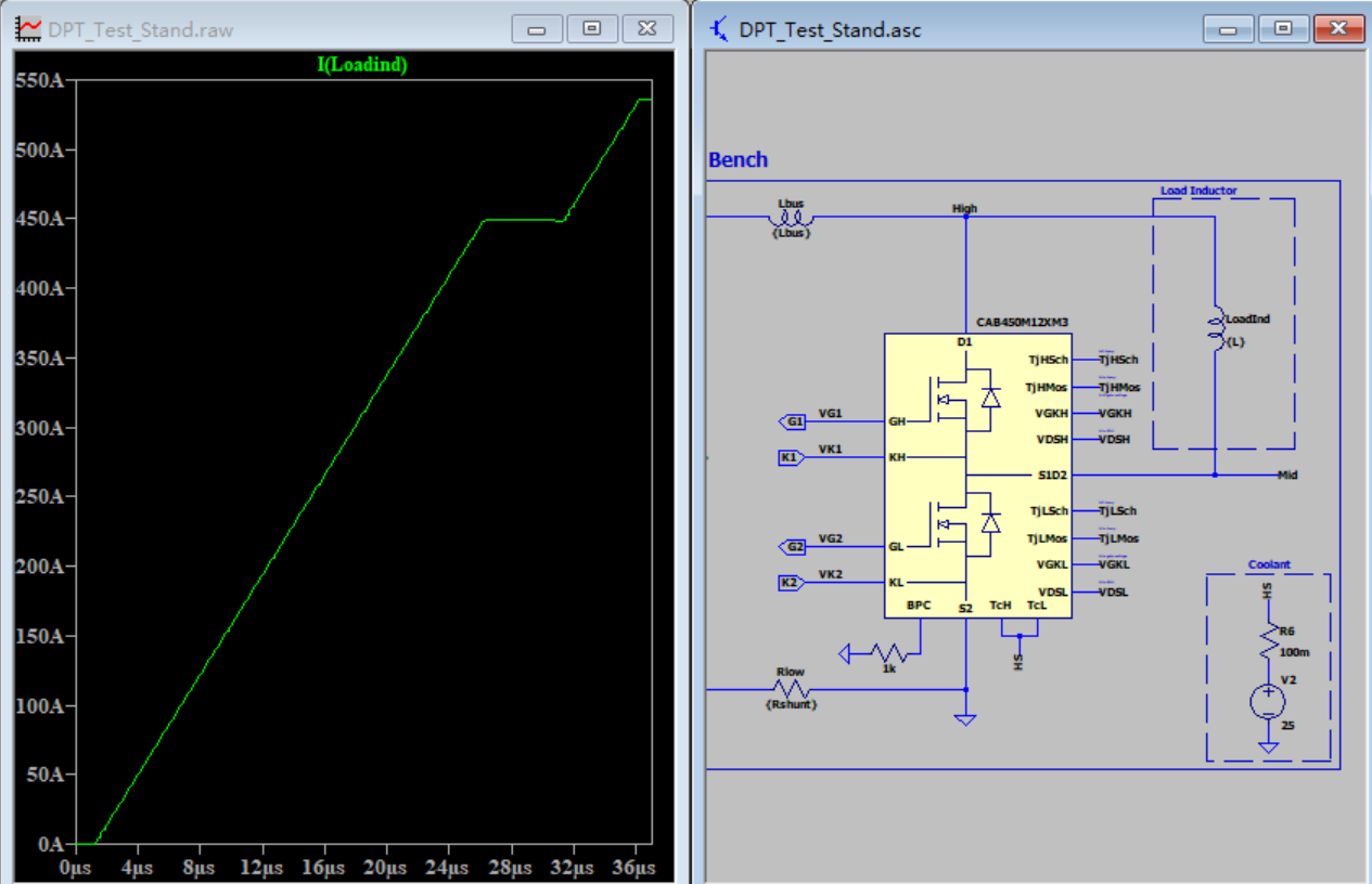
Yes, I have understood what you mean. But I have a question. In the dual-pulse test simulation provided by your company, the previous switching cycle is set to 25us. During this period, the load current continues to rise. The load current flowing through the upper tube diode will exceed the specified 225A for more than ten us. Is this reasonable?
0 -
I was wrong. What I should ask is: after the load current reaches 450A, the lower MOSFET is turned off, so that the 450A current continues to flow in the freewheeling diode of the upper MOSFET. The duration of this period is up to 5us. Can the body diode withstand such a large current for such a long time?
0 -
Hello, can I answer this question? When high-power modules such as the CAB450M12XM3 operate at high currents (such as 400A), their continuous flow time is very long. For example, in the LTSpice model provided by your company, the dead time after the upper tube is turned off is set to 5 microseconds, so that the 400A current originally flowing on the lower tube can be converted to the upper tube. In this way, the current borne by the body diode of the upper tube will be a 400A current of 5 microseconds. Can I use it this way? Because there are similar situations in my project, I hope to receive your guidance.
0 -
Hi baiyujing,
The current limit of a device is dictated by its junction temperature. Higher current results in higher conduction losses, and therefore a higher junction temperature. Thus, ampacity limitations are a function of both the current through the device and the duration of the pulse. The 450A current rating of the CAB450M12XM3 power module is a continuous power rating; as long as the baseplate is maintained at 25C, the junction temperature of the die will not exceed 175C at this current level. However, the module can handle much higher current levels for a short duration.
In the CAB450M12XM3 datasheet (https://assets.wolfspeed.com/uploads/2020/12/CAB450M12XM3.pdf), Figure 18 provides a set of current/voltage limitations for various pulse widths. For example, with a case temperature of 25C, the module can withstand a 1 ms drain-source voltage of 10 V with a drain-source current of 1000 A. You may also find Figure 20 and Figure 22 helpful in understanding the rated power limitations of the XM3 power module.
For the LTspice model, you can observe the predicted junction temperature of the device through the TjHMos/TjLMos ports. This should help you understand the power levels and pulses that are reasonable for your design. However, please note that no simulation will perfectly predict a real system's behavior, and your design should always follow the datasheet recommendations.
Thanks,
Brian
0


