Determination of Internal Gate-Source Resistance Value in Power Module Design Process
Hello Wolfspeed team, Good day!!
We are currently developing silicon carbide power modules for electric drive systems in new energy vehicles using the EPM3-1200-0017D1 bare chip. Before the design process, we conducted a reverse analysis of silicon carbide power modules used in the market for electric drive systems in new energy vehicles. We found that most power modules have a gate resistor chip connected to the gate of each silicon carbide chip, and different products use different values for the gate resistor.
So, here are the questions:
- Why integrate the gate resistor inside the module, even though it adds complexity to the packaging process?
- How to determine the resistance value of the gate resistor connected to each chip inside the module? Is there a specific calculation method?
- For the EPM3-1200-0017D1 bare chip, some manufacturers use a gate resistor value of 2 ohms for each chip connected in parallel inside the module. Is this value optimal? What is the recommended gate resistor value for the HybridPACK™ Drive package?
Thank you,
Shawn
Comments
-
Thank you for your post, it has been approved and we will respond as soon as possible.
0 -
Hello PCShawn,
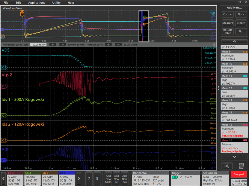
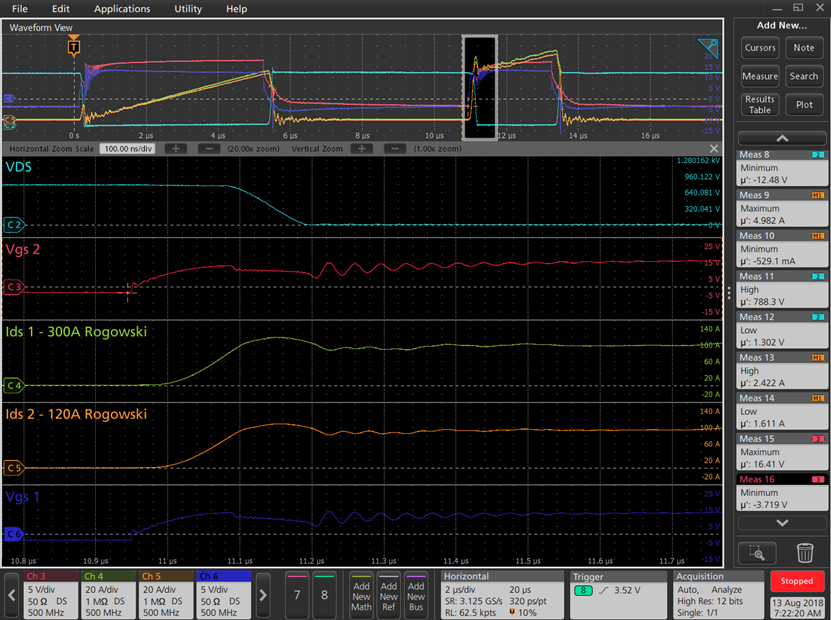
- The gate resistors inside the module are located at each MOSFET's gate to provide damping to the die-to-die interactions that can lead to oscillatory behavior and catastrophic failure of the module. Due to real-world parameter mismatch between paralleled MOSFET devices, an imbalance can occur between die during transients leading to oscillations on the gate network that cause parasitic turn-on and will lead to uncontrolled behavior of the module. Simply adding gate resistance to the outside of the module is not sufficient for damping the die-to-die oscillations; there must be resistance between the die to squash the oscillatory behavior.
- We create specially instrumented modules to thoroughly characterize the dynamic performance of module design and die through double-pulse testing. Accurate VGS waveform quality at various points in the gate/source network is the main focus for this testing.
- To find the ideal resistance, the die & module should be tested and thoroughly characterized across all expected operating conditions to guarantee stability across the entire SOA. The ideal internal gate resistance is the smallest value that adequately damps the die-to-die oscillations across bus voltage, current, junction temperature, etc.
Example of inadequate gate resistance per MOSFET inside a module:
Example of the same module operating at the same switching speed with gate resistance moved inside the power module to damp die-to-die oscillations:
Best Regards,
Austin C.
0 -
Hi, I hope that this answered your question. I will close this discussion for now but if you have a follow up question, please "Start a New Discussion" and we would be glad to support you further.
0


