Questions on Vgs(M)_External vs Vgs(die)_Internal
Hi Wolfspeed Expert
As Wolfspeed claimed the max rating of Vgs is -8V/+19V in the datasheet of CAB530M12BM3, would you kinldy review below questions and address the concern, thanks.
- is there any reliability concern if customer guarantee the Vgs overvoltage within the -8V/+19V at the Vgs(M) testing point? Do we have any data
- Is the Vgs postive/negative overvoltage measured at the Vgs(die) worse than at the Vgs(M)? is there simulation data or measurement data can be proved this assumpation?
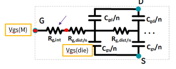
- How to design/select a right Rg(int) from Vgs overvoltage and oscillation point of view for module desgin ? Does it need to de-cap module and do the Vgs measruemnt at the Vgs(die)?
Thanks
Mason
Comments
-
Thank you for your post, it has been approved and we will respond as soon as possible.
0 -
Hi MinC,
Q1
The gate-source voltage at the module terminals should be limited to -8V/+19V (or whatever limit is specified in the datasheet). It is not practical to measure Vgs at the die level of a power module, and thus the rating is specified at the module terminals. All Vgs measurements should be made with optically isolated voltage probes with high common mode rejection. Information from this testing can be used to select an Rg that meets the requirements of the datasheet.
Q2
The answer to this question really depends on far too many factors to give a definitive answer. It will depend on the value for Rg,int, Rg,ext, Rg,dist, parasitic inductance, the layout between parallel die, temperature, etc. There may also be parasitic ringing that is difficult to predict in simulation. However, I will try to provide some general guidance here.
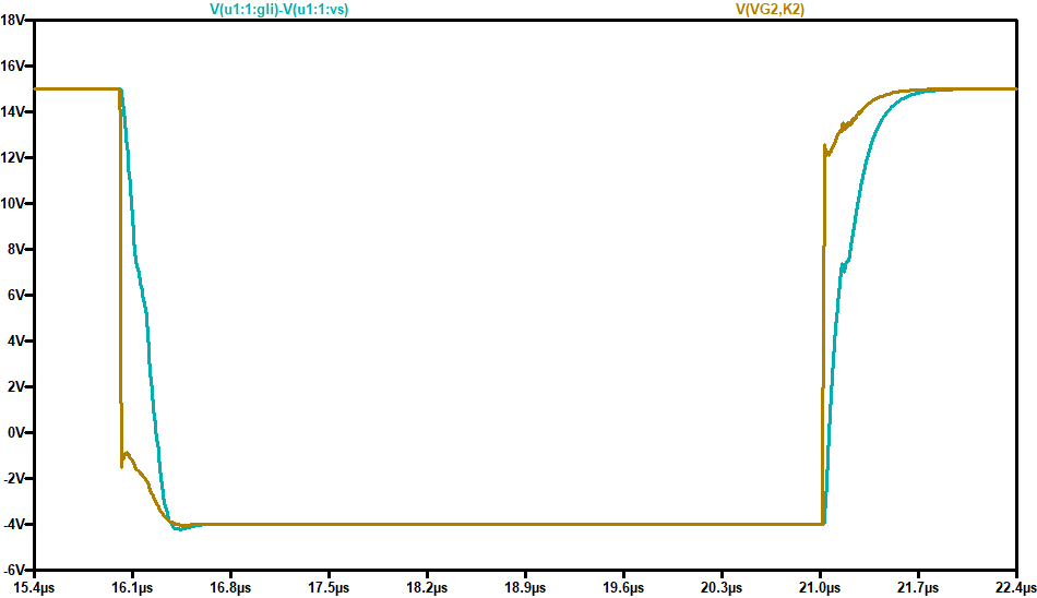
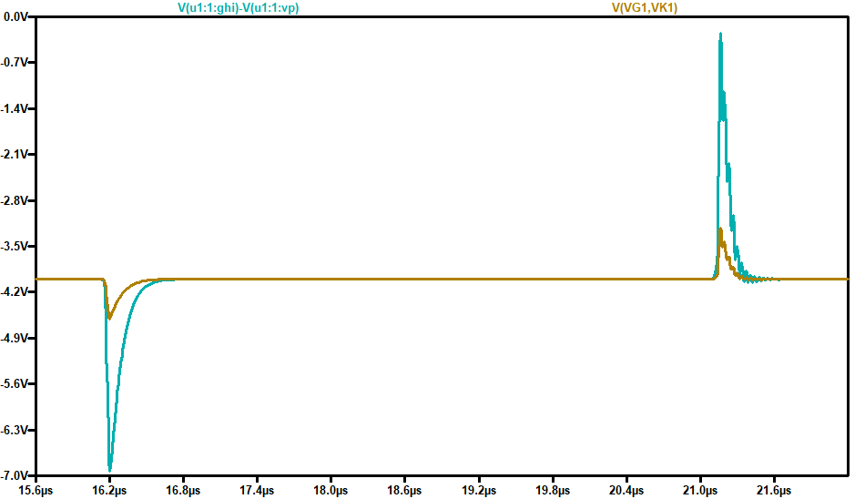
For the active switch, where the primary energy flow is from the gate driver to the die, the VGS overshoot/undershoot will be worse at the module terminals. We can see this in simulation (see below). The gold waveform is the gate-kelvin measurement at the CAB530M12BM3 terminals, and the teal measurement is the gate-source measurement at the die. The die voltage lags behind the module terminal voltage because of the voltage drop across Rg,int.On the other hand, for the inactive switch, the primary energy flow is being coupled from the power loop into the gate-drain capacitance. Here, we see significant higher over/undershoots (see the simulation screenshot below. Teal is the gate-source voltage at the die, gold is the gate-source voltage at the module).
To determine how different the module VGS and die VGS will be, you need to know the module VGS, the gate current, and Rg,int. You can also use simulation to analyze this. I've included an example simulation for the CAB530M12BM3 in the .zip. You will need to go to tools → control panel and enable 'save subcircuit node voltages' (see below).
Q3
Can you clarify this for me? Are we talking about selecting an Rg(ext) for using the CAB530M12BM3 power module, or is this a question about using bare die to design custom modules?
0 -
Then, there are a few approaches to address this. The first approach is to measure the gate-source voltage at the die on their module. However, it may not be practical to attach an MMCX connector to perform a proper measurement (flying leads are not recommended). Another option is to develop a PCB that mimics their module layout, and include gate measurement points at the "terminals" (before Rg,int) and at the die. Since the customer knows their Rg,int value, they could also add a gate current measurement and calculate the VGS voltage at the die through the following:
VGS(die) = VGS(M) + IGS*Rg,int
One method to measure gate current is to use an optically isolated probe to measure the voltage across an external Rg located on the kelvin gate path.
 1
1 -
Hi, I hope that this answered your question. I will close this discussion for now but if you have a follow up question, please "Start a New Discussion" and we would be glad to support you further.
0


