Speedval Kit Daughter Board MMCX measurement
Dear community,
I am studying the speedval kit daughter board's datasheet (e.g. MOD-PWR-MM-...J SPEEDVAL KIT™ TO-263-7 POWER DAUGHTER CARD USER GUIDE). I see that the MMCX connector that measures the Ids is connected in reverse. Meaning that the "positive" signal that is measured is the V_shunt-, and the reference (shield) of the mmcx is the V_shunt+. Is there a specific reason for that?
Moreover, I see on the respective video showcasing the functionality of this kit, than an adaptor from mmcx to bnc is used. Is there a specific reason besides the package of the mmcx that we prefer to use an adaptor that leads to a bnc anyway?
Thank you in advance!
Comments
-
Thank you for your post, it has been approved and we will respond as soon as possible.
0 -
Greetings:
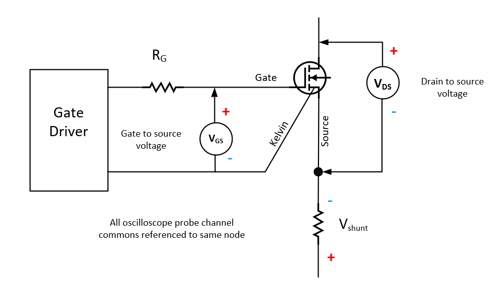
Thank you for your question. The reason the shunt test point has the polarity is reversed is so that all scope channels references or commons are tied to the same node. Connecting the commons for VDS, VGS, and IDS(shunt) is ideal for signal fidelity and avoiding ground loops.
The reason the MMCX connector is used for sensing gate and shunt currents is the small footprint makes it ideal for pcb layout with minimal insertion inductance. The shunt voltage and gate voltages are low voltage (<25VDC) so MMCX connectors are more than capable of handling the requirements.
.
 1
1 -
Thank you for the answer!
So the bandwidth has nothing to do with the selection..
I am reading a random mmcx that has an insulation of 6kV. Is there something I am missing about the voltage readings? Can we use an mmcx for measuring Vds levels up to 100V or 200V?
I am not capable if distinguishing it on the datasheet, but, every IC will have a reference to the V_shunt+ (or half-bridge middle point), right
0 -
The bandwidth of both BNC and MMCX connectors are typically in the 2-6 Ghz range which is more than enough bandwidth to capture waveforms on SiC. BNC connectors are physically larger and have more spacing/creepage between the signal and common pins which makes them more suitable for the higher voltage requirements for VDS measurements.
All Speedval daughtercards come equipped with current shunts only on the source of the bottom MOSFET therefore the shunt, as well as VDS, and VGS for the bottom MOSFET will be referenced to the -DC bus not the midpoint.
 1
1 -
Even though the voltage drop on the shunt(s) will be small, wouldn't it be better if the gate driver had as a reference the source of the bottom MOSFET, as well as the isolated power supply, and any digital isolators? If these have a reference to -DC, the gate driver's output signal V_gs on the bottom MOSFET will have a slightly wrong voltage reference, no?
0 -
The gate driver is actually referenced to the source (Kelvin) of the bottom MOSFET. I attached another image to hopefully clarify.
 1
1 -
Hi, I hope that this answered your question. If you have a follow up question, at a later date, please "Start a New Discussion"
 1
1


