SPICE model for discrete devices
I would like to inquire whether the parasitic parameters provided in the SPICE model for discrete devices, such as Ls1, Ls2, and Lg, include the long leads of the discrete device, or if they only account for the path from the die to the root of the pins. Additionally, in practical use, is the loop inductance contributed by discrete devices generally larger or smaller than the values in the model? According to the parameters extracted from finite element simulation (excluding the device) and double pulse test results, it seems that the total inductance of the C3M0021120K is around 12nH. Could you confirm whether this is reasonable?
Comments
-
Thank you for your post, it has been approved and we will respond as soon as possible.
0 -
Hello,
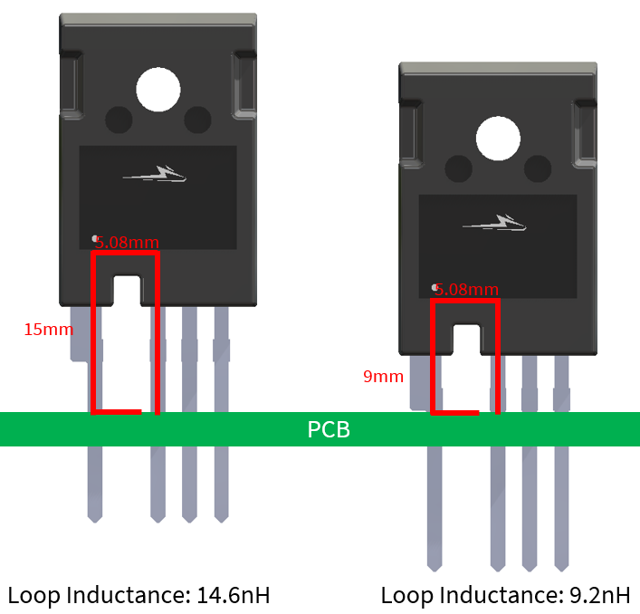
Thank you for your question. The inductance of the power loop (drain to source) is a function of the lead length from the package to the PCB, the connections on the PCB to each terminal, the wirebond scheme in the package, and the die location in the package. The model is intended to capture the device parasitics including the wirebonds and the minimum lead length. The specific part you are asking about has a total power loop inductance of 8.32nH in the model. This matches closely with a simplified analysis of the loop from the PCB to the inside of the package, which shows 9.2nH when mounted in the fully seated configuration as shown below on the right. If the device is not fully seated, the inductance can increase dramatically as shown on the left.
In your case, your analysis of the PCB layout and switching dynamics shows a total package inductance of 12nH, which is also reasonable, but may also reflect some inaccuracy in the model of the other PCB components. Overall, if your goal is to make a parasitic circuit model that matches the switching dynamics, it will require tuning some of the parasitic elements in the circuit, but it sounds like what you have is quite close, and likely sufficient for any further simulation you require.
Thanks,
Adam
 1
1 -
Thank you for your relentless support. In my implementation, the heatsink needs to be parallel to the PCB, necessitating the bending of the leads. Therefore, the actual assembly method is more similar to the one shown in the left diagram you provided, which resulting the increased loop inductance.
0 -
Yes, that makes sense in your case why the inductance is slightly higher.
Please let me know if you have any further questions, otherwise, use the link below to close this thread.
 1
1


