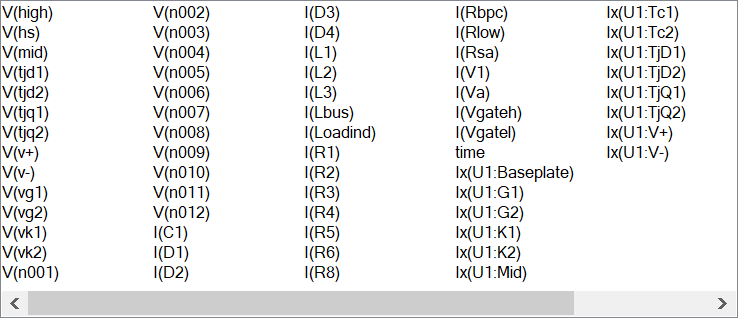
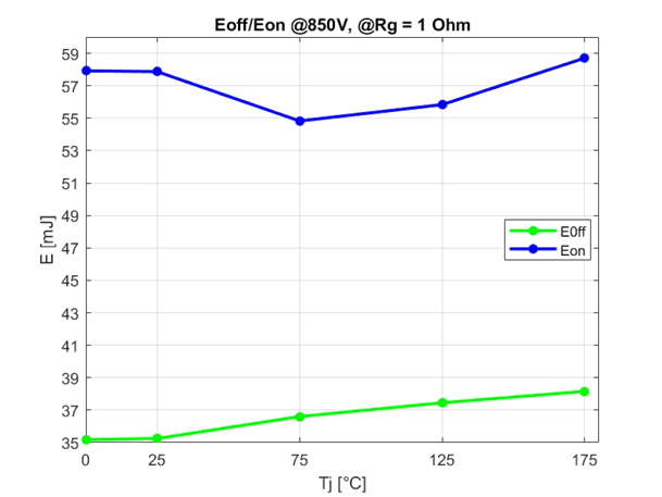
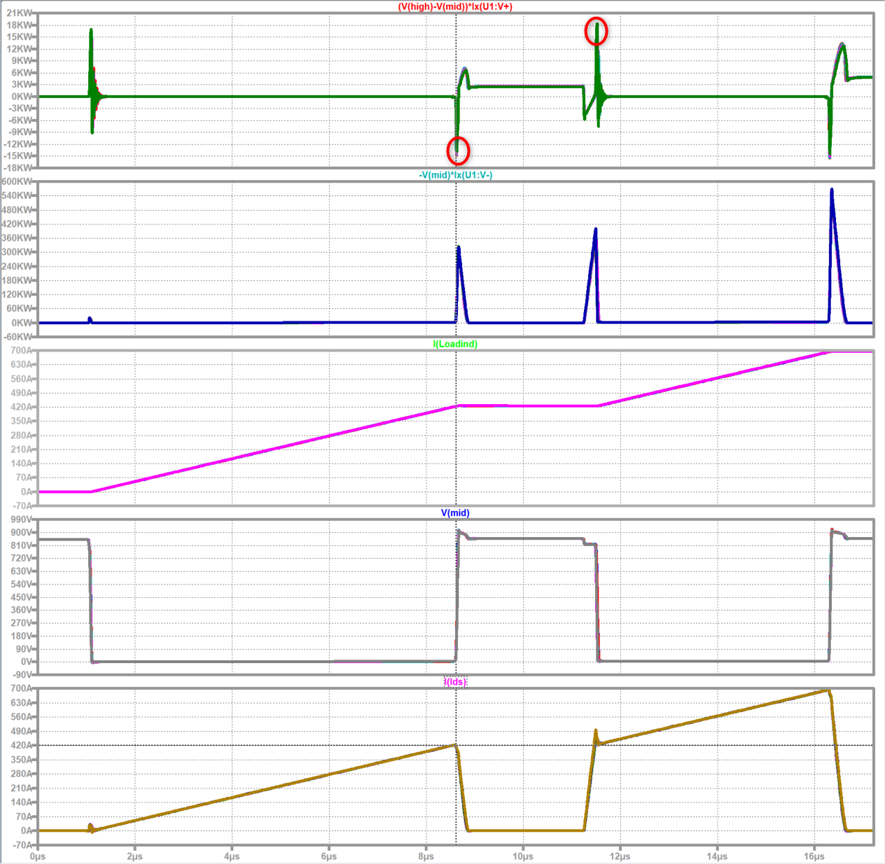
Negative power at Tj sweep 0°C...175°C at DPT
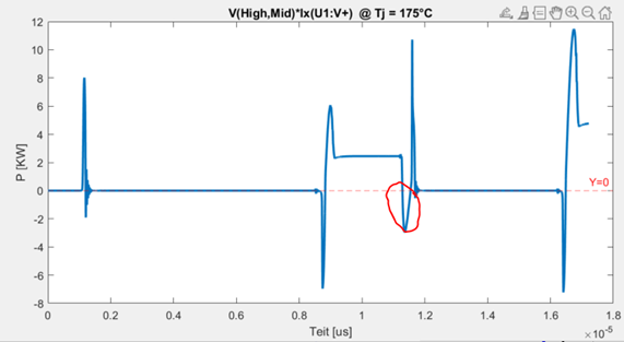
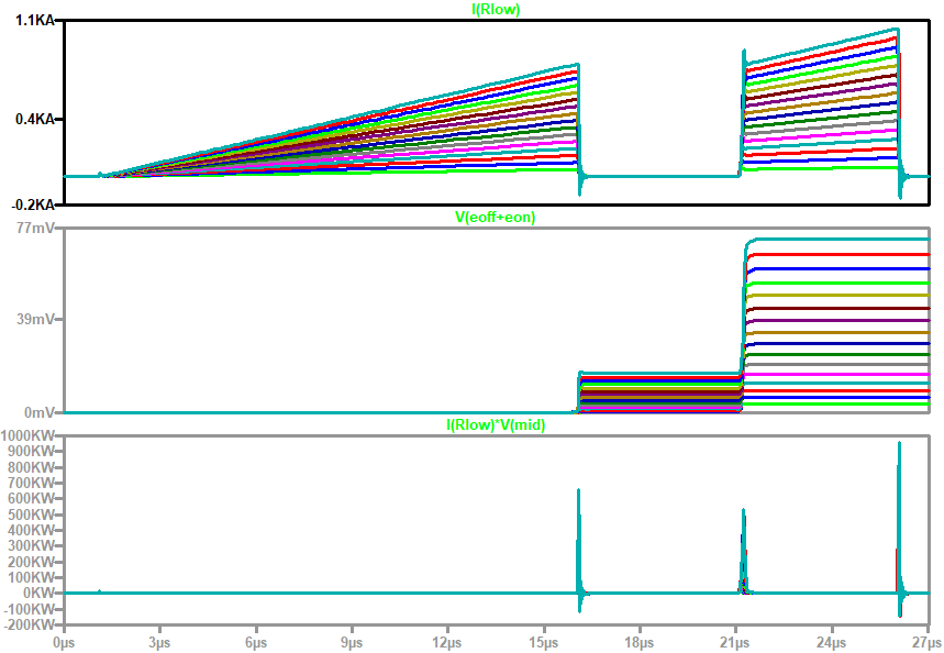
Hello, I don't understand why I get a 0 line shifted downwards at power. This also influences my energy calculat.
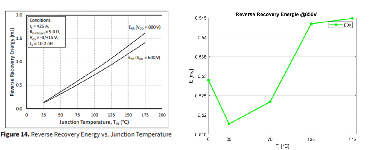
But this cannot be the truth, that with increasing Tj the energy loss decreases.
But if I mathematically shift the negative zero line up to 0KW, I get different energy.
and if I simply calculate Vmid*Ids, the power is not shifted downwards and I also get plausible energy losses.
My question now, which of these three methods is correct? and more accurate. why is the zero characteristic curve in the model equation for power shifted to the negative range where no current flows?
I assume that the calculation of I*U is not as accurate as I take this long equation from Model. Is there an error in the model equation for power or am I making a mistake?
this is the power formula of double pulse test model.
V(N005)*Ix(U1:V+)+V(UDS)*Ix(U1:Mid)+V(N013)*Ix(U1:V-)+V(VG1)*Ix(U1:G1)+V(VK1)*Ix(U1:K1)+V(VG2)*Ix(U1:G2)+V(VK2)*Ix(U1:K2)+V(HS)*Ix(U1:Tc1)+V(HS)*Ix(U1:Tc2)+V(TjQ1)*Ix(U1:TjQ1)+V(TjQ2)*Ix(U1:TjQ2)+V(TjD1)*Ix(U1:TjD1)+V(TjD2)*Ix(U1:TjD2)+V(N012)*Ix(U1:Baseplate)
I would like to use the model equation, I think it is much too accurate, because it has many dependencies in it, which corresponds to reality.
Comments
-
Thank you for your post, it has been approved and we will respond as soon as possible.
0 -
Hello,
I would not use the LTspice power formula on the module block - all that formula is doing is looking at the power flowing in/out of all of the module pins and calculating it as "power." However, many of the pins in the model aren't even electrical (for example, the temperature pins), which will cause major problems.
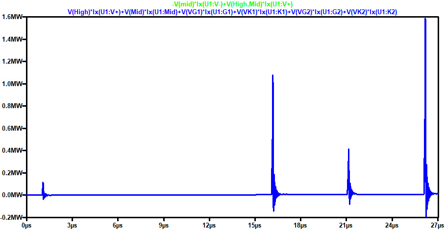
There are a few ways you can get power. I recommend looking at the measurements from outside the module and not worry about internal measurements. For example, if you want the power across the low-side switch, you could use the equation:
eqn1: -V(mid)*Ix(U1:V-)
For the power across the high-side switch:
eqn2: V(High,Mid)*Ix(U1:V+)
Now, if you want to use that power equation from LTspice, you just need to remove all the references to the Tj/Tc/baseplate pins:
V(High)*Ix(U1:V+)+V(Mid)*Ix(U1:Mid)+V(VG1)*Ix(U1:G1)+V(VK1)*Ix(U1:K1)+V(VG2)*Ix(U1:G2)+V(VK2)*Ix(U1:K2)
This equation gives the same result as eqn1 + eqn2 above.
I suppose this would represent all power losses in the module, but again I recommend just looking at the high-side/low-side switches separately as shown above.
Thanks,
Brian
0 -
Thank you very much.
I want total losses. To understand in case it is low side switch DUT in DPT test, then losses of high side switches corresponds to losses of body diode only correct?
In LT Spice simulation, there is no node with name V(High,Mid) which is in equation 2 in your explanation.
Can you say which node you mean exactly.0 -
Hello,
Yes, your understanding of the losses is correct.
V(High,Mid) is simply V(High) - V(Mid) (node names are not case sensitive in LTspice).
0 -
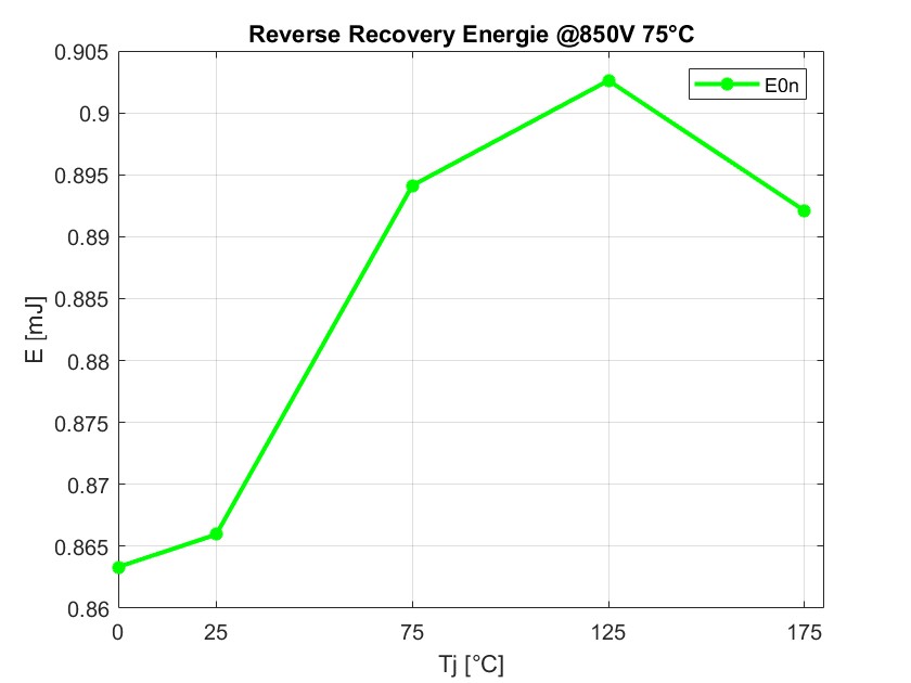
I am in the process of calculating the Reverce Recovery Energy.
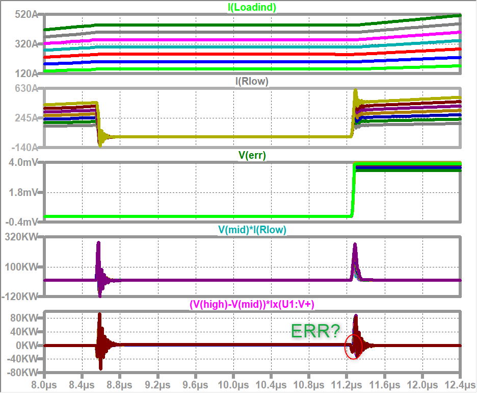
To do this, I use the power curve V(High,Mid)*Ix(U1:V+) and calculate the energy from this.Here is the power for Tj=175°C. I then take the amount of area under the marked point.
That I do fot Tj 0, 25,75,125, 175
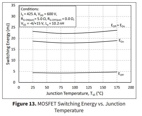
When I compare with the plot from the data sheet, I don't get as strong an increase as in the data sheet. Could you tell me what could be the reason.
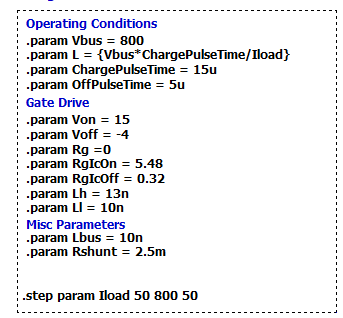
I use almost the same parameters as in the data sheet
Rgon =5Ohm
Is =420A
Vgs = -4/15
Lstray = 5nH (with 10 nH looks the same)
Thanks!
0 -
Hi there,
I'll need some more info to help you out. Could you show me some screenshots of your circuit and how you've configured it?
Thanks,
Brian
0 -
hello Brian,
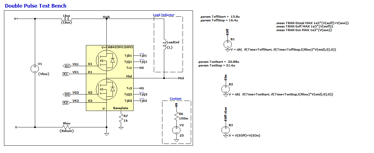
I use this setup. The data sheet says Lstray =10nH.
I have simply split this between both switches so I have LcsiQ1 and LcsiQ2 4nH.
I get much too high switching energy than in the data sheet, which I can't explain. although I use Rgext 1 Ohm and not 5Ohm as in the data sheet. This means that if I also use Rg = 5 ohms, I get even greater energy loss. But the tendency looks to be correct.
if I get much too much switching energy , then the energy loss should also be much higher or not the other way round smaller?Thanks!
0 -
and I use your recommended equations for power calculations.
Is normal for body diode to see so big power peak?
Thans
0 -
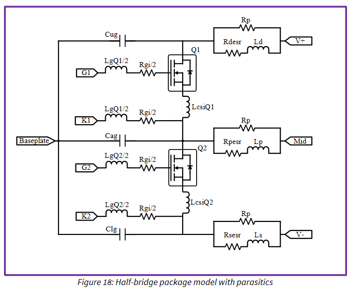
So, I see you have set LcsiQ1 and LcsiQ2 in the spiceline of the model. This is not correct - those are common-source inductances of the module. These will substantially increase the switching losses of the device. Two comments here. One - if you were to change the stray inductance of the module, you would be interested in Ld and Ls in the below circuit. Two - you do not need to specify the stray inductance from the datasheet, because it is already included in the model. Please remove the 'LcsiQ1' and 'LcsiQ2' definitions and let me know if the switching loss agreement improves.
Some other feedback:
- Rather than passing 'Tj' through the Spiceline, it is easier to change the .TEMP variable. For a sweep, you can do .step param TEMP list 25 75 175 etc.
- I see you added a parallel RLC network - this won't have any effect with the voltage source V1 placed in parallel. I recommend just deleting the RLC, but if you want to keep it, you can delete the voltage V1 and use a .ic command to initialize the voltage across the capacitor.
Please make these changes and let me know if it solves some of your issues. I'm seeing a clear trend in ERR and temperature from my simulation.
Thanks,
Brian
0 -
Hello Brian,
I also sweep LcsiQ, Ld and Ls.
So far I have proceeded as follows.
I have defined desired parameters in Spiceline (e.g. LcsiQ2 = {LcsiQ2}and then .step param TEMP list 25 75 175 etc.).All other parameters are unchanged.
I did the same for Ld and Ls. Is this correct, or should I pay attention to something else?But as far as the Eon and Err are concerned.
I have implemented all their types. Removed capacitor, removed LcsiQ1, LcsiQ2 and Tj from spiceline and instead of Tj, I vary TEMP.Now I get almost twice as big Eon and Err as before.
I think something is wrong here.
Thanks.
0 -
Hello Brian,
Can you please tell me how you calculate your Eon/Eoff and Err? What areas of performance do you take into account exactly?
Thanks!
0 -
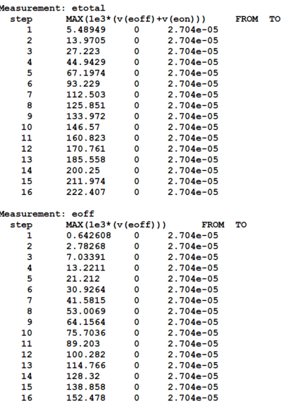
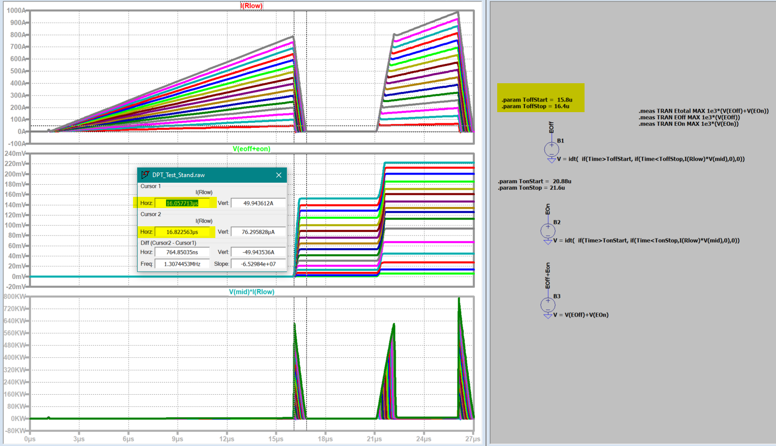
So I'm not sure what's going on with your switching loss values, but let me provide you a baseline to work with. See the attached circuit file. I added some switching loss measurements to the right. I've also included some options to sweep the load current to follow some of the DS plots.
For the gate driver, I've hijacked the RgIcOn and RgIcOff to follow the 5 ohm on / 0 ohm off from the datasheet
Below are what the waveforms look like from my end. Make sure you have LTspice's default solver settings applied (Tools → Control Panel → SPICE → Reset to default values).
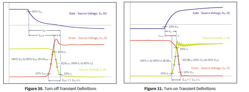
In the simulation, we are calculating switching losses by integrating a wide range around the switching event. This is okay because simulation doesn't have any measurement errors to deal with. In datasheet testing, we follow the below waveforms to extract switching loss.
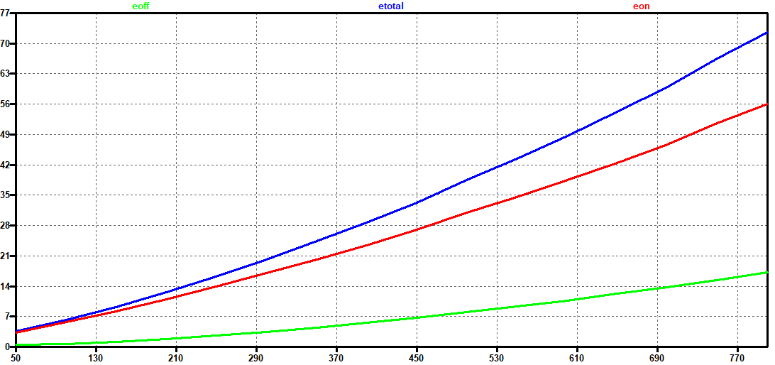
Here are the results from my simulation sweep, which match quite closely to the datasheet
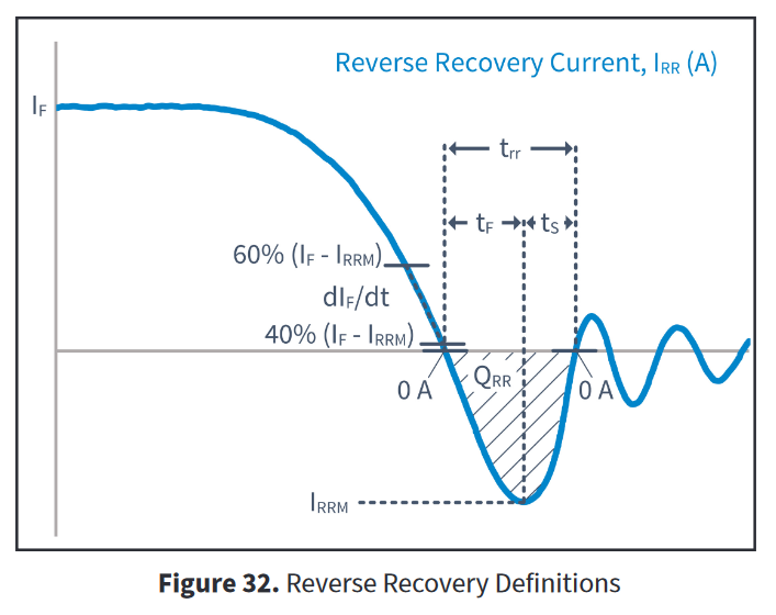
Also - there is nothing odd about that level of power dissipation in the diode. It is over a very short time duration so the overall energy loss is low. You'll want to follow this definition to calculate ERR (find the 0A/0A limits, multiply IRR*VRR, integrate between 0A/0A limits)
Hope this helps.
0 -
Sorry, my switching energy plot never attached.
0 -
Hello,
Thank you, this is very helpful for me.
1)
I am trying to plot the Eon Eoff and Etotal, but I notice that the start and stop times are not being taken over.Stop and start times are defined in your file for Eon and Eoff calculation. I expect these times to be taken into account for .meas TRAN Etotal MAX 1e3*(V(EOff)+V(EOn)).
But as I can see in Spice Output Log File is not the case. The calculated energy refers to the total time.How do you create your plots of Eoff, Eon and total?S
2)
Also, I don't understand why you chose Toffstart = 15.8us and ToffStop= 16.4us. In plots give different values or do I have a mental error?
3)
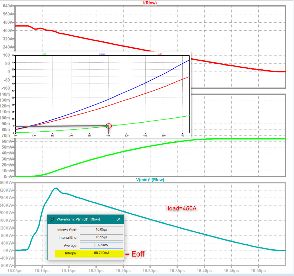
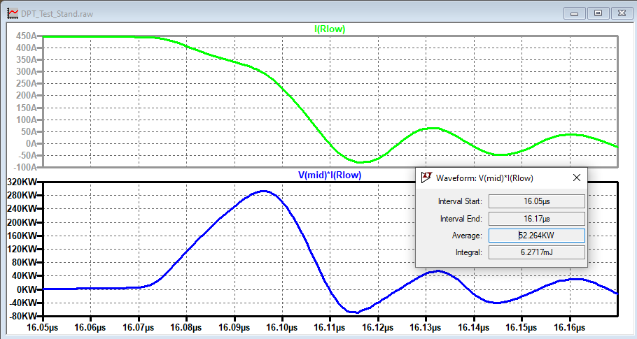
If I integrate the power curve in LTSpice then I probably get a larger value (factor 10) than in your plot for Eoff.
Thanks!
0 -
- In this statement, we are adding the results from the Eon behavioral voltage and the Eoff behavioral voltage source. The time integration bounds are already handled by those sources.
2. I select integration limits very far before and after the switching pulse so that the entire curve is captured across all the .step sweeps. You can change these limits to be more narrow, but it shouldn't make much of a difference because the conduction losses are quite small compared to switching losses.
3. Your waveforms look very different from mine:
Could you send me your simulation file, symbol file, and .lib file that you are using to produce those results?
Thanks,
Brian
0 -
Hello Brian,
I have found why our results did not look the same. My libfile was changed, I have now reloaded.
I get the same results as you.
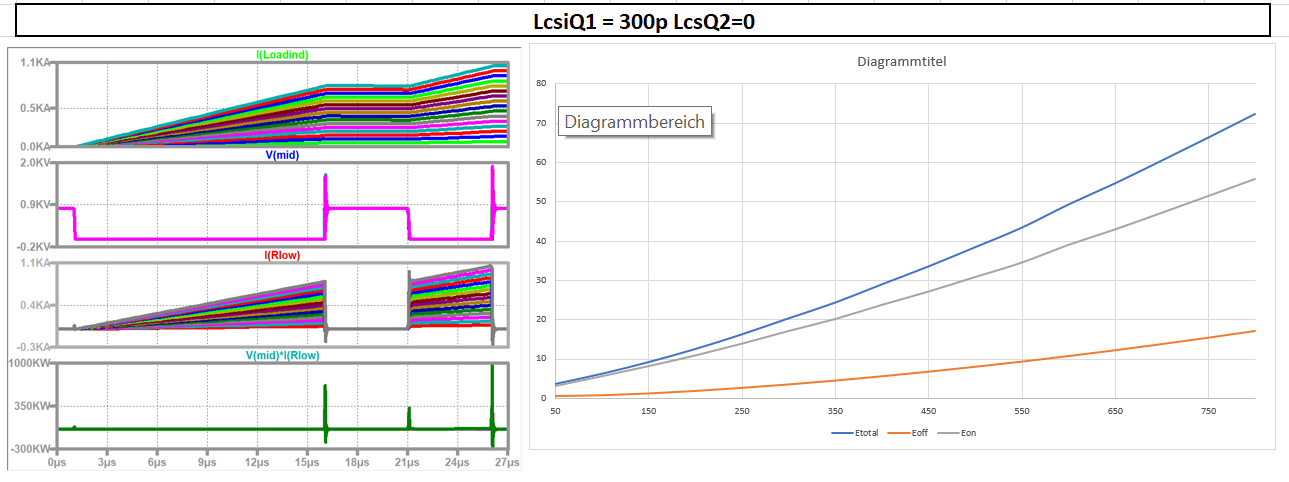
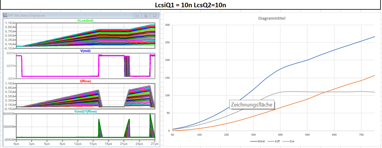
However, only with LcsiQ1=300p and LcsQ2=0. Why do you make assumption with these values? These are not real values, are they? I assume that LcsiQ2 is greater than 0.
If I read Lσ =10.2nH in the data sheet, then LcsiQ1=10n and LcsiQ2=10n, right?
If I apply these values, then I get completely different results. Much larger values for Eon and Eoff.0 -
Hello,
LowSide switch and highside switch are actually the same components, so they also have the same Lstay or not?
As far as Err is concerned, Irr corresponds to Ix(U1:V+) and VRR is equal to V(high)- V(mid) or not?
The command .meas TRAN ERR MAX 1e3*(V(ERR)) cannot be calculated with these variables.
Or do they calculate differently?
I am looking at marked point in plots to calculate Err.Thanks!
0 -
Hi there,
LcsiQ1 and LcsiQ2 are not the same as the stray inductance. The stray inductance in the datasheet is Ld + Ls in the below circuit. You shouldn't have to change any parameters in the model to match the datasheet. LcsiQ1 and LcsiQ2 are different because of some mutual coupling effects within the module, and it is correct that LcsiQ2 is zero. I must repeat that LcsiQ1 and LcsiQ2 are not stray inductance, but instead a common-source inductance. These inductances form a shared path between the power loop and the signal loop, thus the large di/dt from the power path will induce a voltage on the signal path. For example, if you put 1 nH on LcsiQ1, and the di/dt is 10 A/ns, then you will see 10 V induced on G1/K1 - this has a huge effect on switching behavior.
For reverse recovery, if you want to match the datasheet, you will need to switch the high-side (Q1) and put the load inductor on the low-side. Then, you measure the low-side current and voltage and multiply them to determine PRR. Then integrate between the two zero crossings of the current to determine ERR.
Note: I had difficulty using the pin currents in calculations as well. You can always insert a very small passive component (like a 1 uΩ resistor) to measure current.
Let me know if you have any trouble calculating ERR.
Thanks,
Brian
0 -
Hello Brian,
This means that if I want to change Lstray, I can proceed as follows.
Lstray=Ls+Ld.
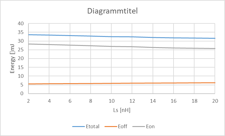
Then I set one of both to zero, for example Ld=0 and let Ls vary by defining Ls={Ls} in Spiceline2 and then using the .step param Ls… command, do I understand correctly?I did exactly like this and I get these results.
Is it plausible that Eon gets smaller with increasing Lstray? I can't explain why, larger Lstray should have a good effect on switching energy.
Also, I can't find any information in the data sheet which inductance is meant by Lσ=10nH.
0 -
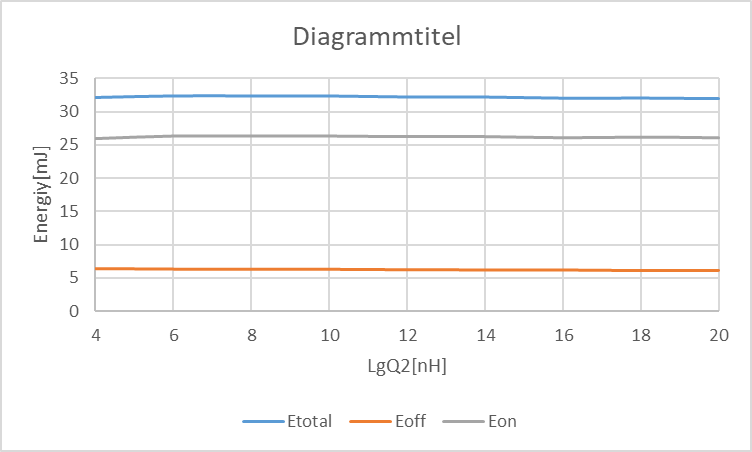
The result for LgQ2 is the same. Does this mean that Lstray and LgQ2 have almost no influence on switching energy?
Thanks
Nugzari
0 -
The primary effect of commutation inductance is on voltage overshoot. Your ability to switch quickly (high di/dt) is limited by the inductance of the system because of V = Ldi/dt. It has limited influence on the actual switching losses of the device. Your gate resistance is limited by this voltage overshoot (as you may have to increase Rg to keep the device in its safe operating area - and increasing Rg will increase SW loss).
But, yes - it's not surprising that your sweeps of these inductances is having very little effect on the overall switching loss. Also, the 'commutation inductance' describes the total loop inductance in the high frequency power path, so in your DPT circuit it would include Lbus as well (but the contribution of just the module is Lsigma).
One thing to keep in mind is that, when you measure voltage at the module's terminals, you are not quite measuring the voltage at the die. To understand this, try this exercise:
Measure V(mid) and V(mid,vk2)
Sweep Ls
V(mid) should remain about the same, but V(mid,vk2) will change quite a bit. This is because, when you measure from the module terminals, any inductance in that measurement path is effectively ignored.
Thanks,
Brian
0 -
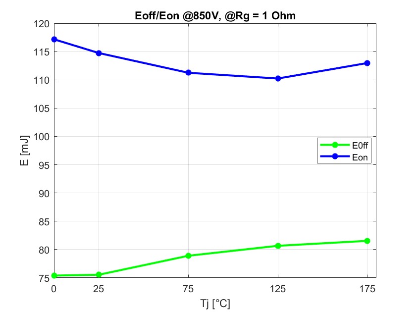
It cannot be true that the switching energy decreases as L increases. Where is the error? This time it can't be the .lib file. This is the same file as for Iload Plot, for example. I get the same values as you and that is plausible.
This plot sweep Lbus between 10nH and 50nH.
My setup looks like this
My setup looks like this, I haven't changed much. Iload=425A. Vbus=850V
Pulse duration 7.5us and 2.7us but these changes have no influence on switching energy.Lstray and LgQ2 Plots are also with same Setup make.
Can you explain why the energy behaves like this with increasing L?
0 -
Unfortunately, I didn't understand what they meant by Err and how I should proceed.
Can you please explain in more detail.Thank you.
0 -
Hello,
It's actually not unusual for higher bus inductance to have lower switching losses. Here is a paper I've found that shows the same trend:
Higher bus inductance will result in greater voltage overshoot, which will reduce how quickly you can switch the device while remaining within the voltage specification - this is the primary disadvantage of stray inductance in a power electronics system.
Thanks,
Brian
0


