SIC MOSFET (C3M0280090J) Used in Flyback Converter Drain to Source voltage stays 20V when switching.
Hi,
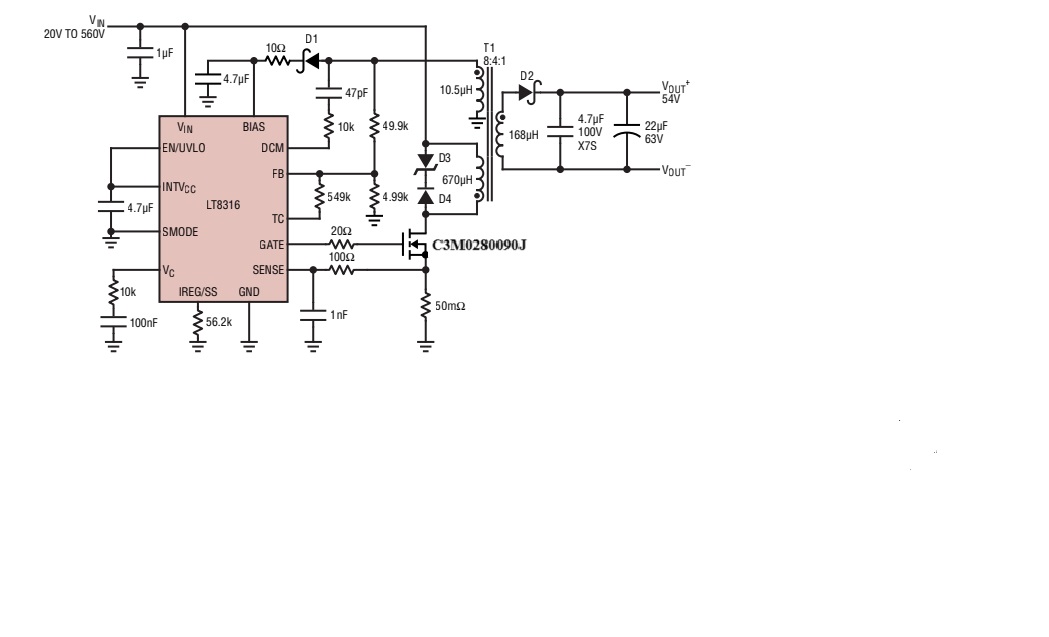
I am using SIC MOSFET (C3M0280090J) in my Isolated Flyback Converter.
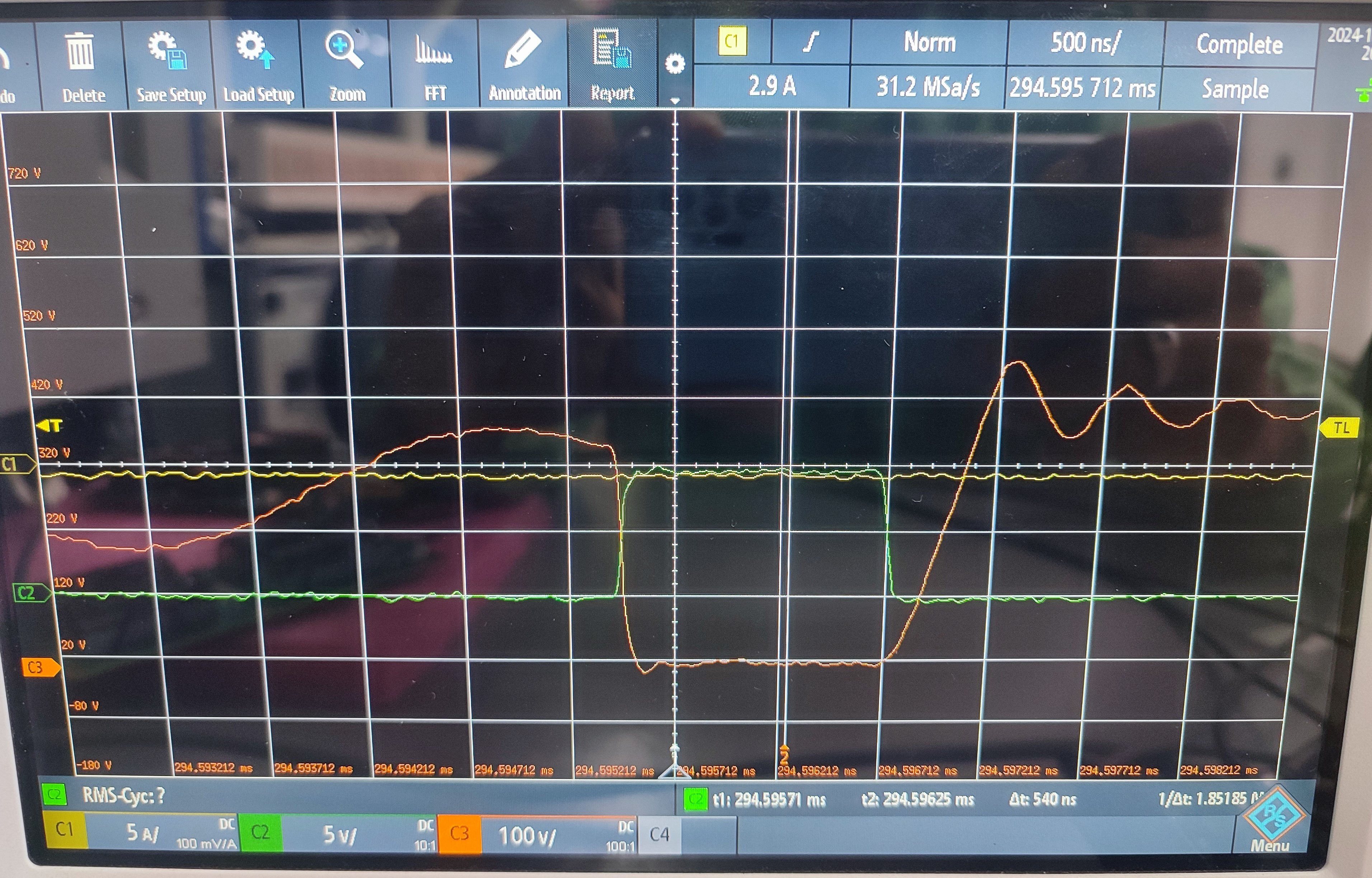
In that I have facing one problem. When MOSFET switches, Drain to Source stays in 20V instead of 0V even though Gate of MOSFET is 10V. I have directly probed across MOSFET because I have used isolation trans
former at input.
I have attached my schematic and observed waveform for reference.
Kindly suggest solution for above problem.
In waveform,
Green - MOSFET Gate Orange - Vds of MOSFET
Thanks,
Vignesh.
Comments
-
Thank you for your post, it has been approved and we will respond as soon as possible.
 1
1 -
Hello,
Thank you for your question. There are a couple considerations here. From a planning perspective, I want to make sure you are aware that the C3M0280090J has recently been announced as moving to last time buy status, and is not recommended to use in a new design. Recommended replacements are the C3M0160120J or C3M0350120J which are drop-in compatible devices with a higher blocking voltage.
From a technical standpoint, the points mentioned below would also apply to the recommended replacements, so it still makes sense to troubleshoot what you are seeing.
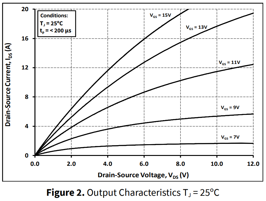
- The C3M family of MOSFETs are intended to be driven with Vgs=15V. At 10V, the device is not fully turned on, and will have higher Rdson. This can be seen in Figure 2 in the datasheet. This will lead to a higher voltage drop across the part and increased dissipation. Operating at 10V may also result in increased part-to-part performance variation in Rdson.
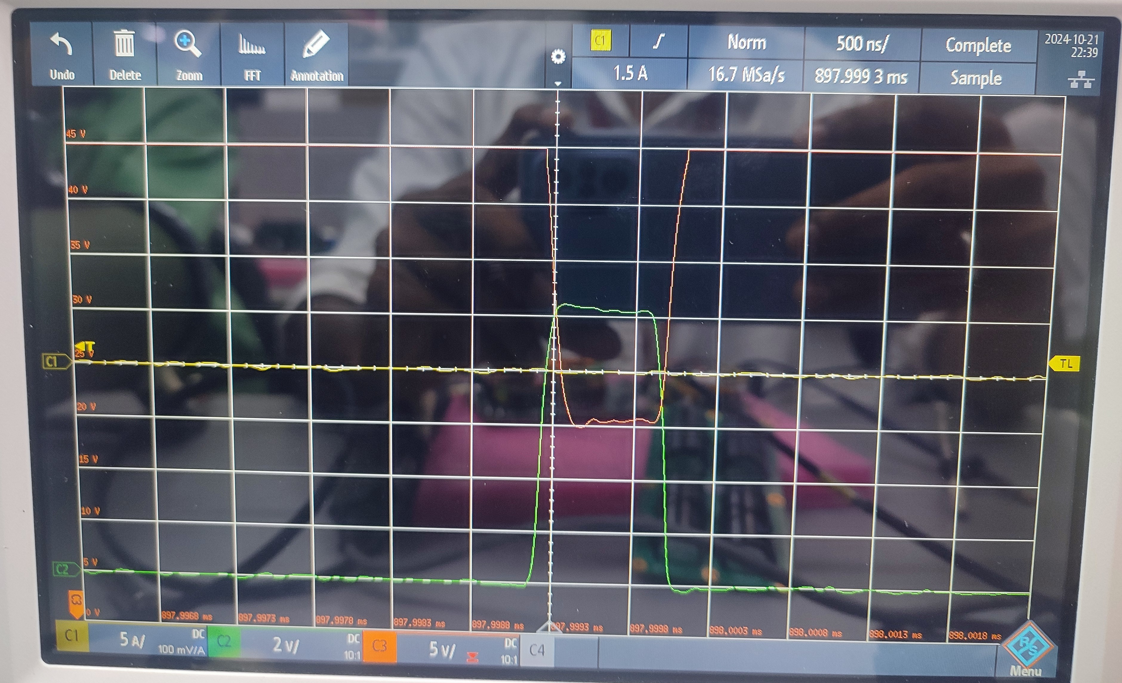
2. The scale on the scope makes it difficult to accurately see the Vds reading. I'd suggest getting a capture with the scale set to 2-5V per division to get a more clear look at the on-state voltage. Obviously this will clip the waveform in the blocking state, but for the purpose of this investigation, that is ok.
3. What probe is being used? Check the accuracy and offset specifications as many high-voltage differential probes can have significant offset.
If you can share an updated image from #2 and include a current trace as well, that will help with further analysis.
Thanks,
Adam
0 -
Hi Adam,
- In circuit Switch current is about 0.35A by looking at graph for Gate to source of 10V, Drain to source voltage is nearly about 1V then how 20V is observed?
- I have attached waveform for your reference for a scale of about 5V.
- I have tested with high voltage probe (100:1) and then i have checked with (10:1) probe the same 20V observed in Drain to source.
Kindly suggest solution ASAP.
Regards,
Vignesh.
0 -
Hello Vignesh,
Thanks for the updates. Can you share a few more details?
Are the Vds and Vgs probes connected directly to the mosfet source, or are they connected to the circuit ground?
Are all of the circuit values the same as shown in LT datasheet diagram you attached? Especially the shunt resistor and the Rg.
Do you get the same waveforms if you only have 1 probe connected to the circuit at a time (eliminating potential ground loops)
How are you measuring current? Can you add a trace to the scope showing current?
Ultimately as I noted above, the parts are not recommended to run at 10V, and the behavior will be less predictable there. The datasheet V/I curve is for a typical part. These curves vary from part to part, and the low Vgs cases will change the most.
0 -
Hi Adam,
Thanks for your reply!
I have previously mentioned that I have directly probed across MOSFET because I have used Isolation Transformer at Input.
R shunt resistance values is around 0.28 ohm for that resistance switch current is about 0.35A.
I have probed MOSFET drain to source alone but same 20V observed.
I won't measure switch current, I have simply inform you that sense pin voltage is around 100mV in LT8316 and sense resistance value is 0.28 ohm by that calculating current is around 0.35A.
Why this part is not recommended to operate 10V Vgs because by looking at graph for Vds & Ids (with Vgs) then only I have used this MOSFET.
Kindly suggest solution as soon as possible.
Thanks,
Vignesh.
0 -
Why curves vary from part to part, then how we chose this part is acceptable for us or not.
0 -
Hi Vignesh,
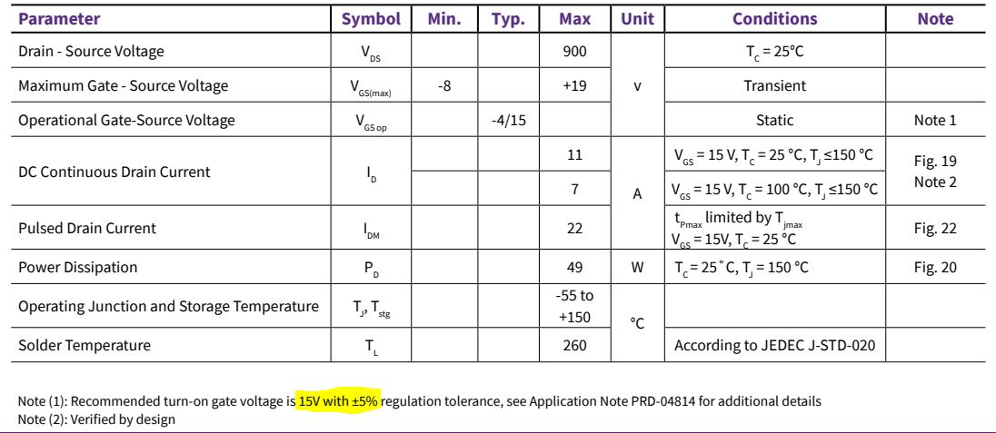
The datasheet notes on the first page that the on-state Vgs is recommended to be 15V+/-5%.
Operation below this level starts to operate the device in the linear region. These parts (and all SiC MOSFETs on the market today) are not designed to operate in this region, and are only intended to be gated fully on or off. You can see in the IV curves that at low Vgs voltages the curves become very flat indicating that the voltage drop will continue to rise with very little additional flowing because the device is in saturation. The exact relationship depends heavily on the Vgs-Vth applied as well as the transconductance gain of the device. The curves are provided to assist in modeling and understanding device behavior as the device is switched on and off and passes through these lower Vgs regions, however, continuous operation at these points is not recommended.
As with all semiconductors, there is a distribution of parameters such as Rdson, Vth, and transconductance in production. Since the devices are intended to be operated at 15V, the Rdson is only guaranteed and tested in production at this level. We do not recommend using this device with Vgs=10V as we cannot guarantee reliable operation in this region.
0 -
Hi, I hope that this answered your question. I will close this discussion for now but if you have a follow up question, please "Start a New Discussion" and we would be glad to support you further.
0

