How to correctly determine device power dissipation
Hi
I am new to power electronics. I am working on a forward converter design with high side active clamp. It is based around the LT3752-1. See attached LTspice model for the primary side using the Wolfspeed parts. (This is not complete, trying to understand device switching parameters)
The datasheet for LT3752-1 (pg40) describes determining the MOSFET total power dissipation as = Pconduction+ Pgatedrive + Ptransition. I get a total of 1.8W for this based on the operating parameters and using C3M0075120J. Based on this low dissipation heat-sinking was limited to a 2oz 4layer stack of area 24mm x 12mm. This also connects to the TX primary windings.
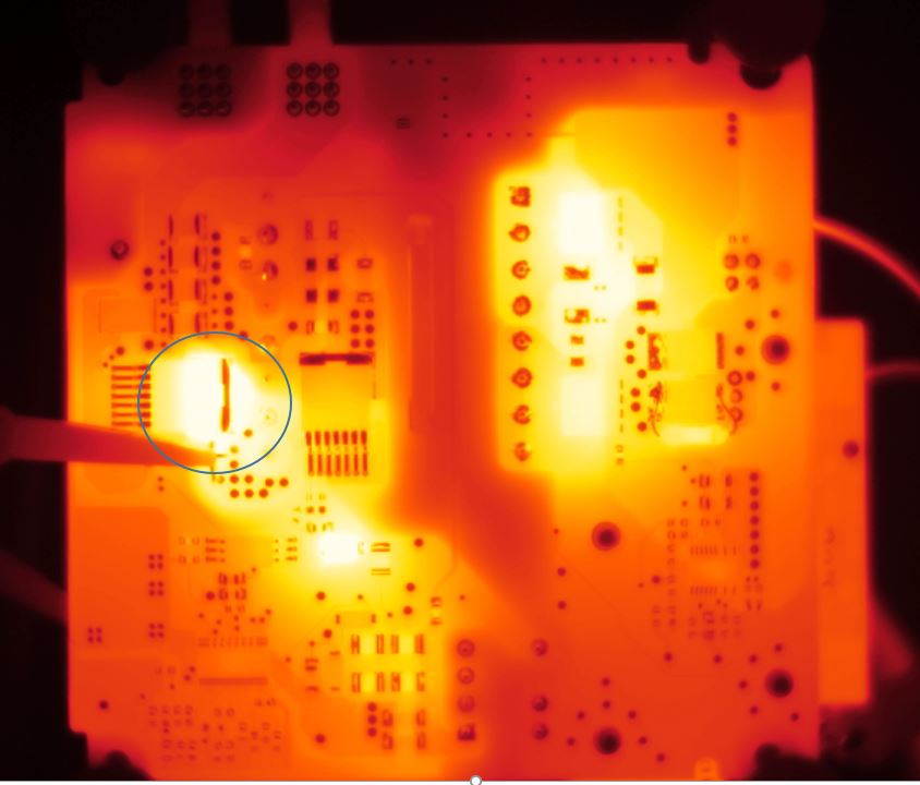
When running under load for approx 4min we observed the following heating profile on the board:
Circled part is main switch and had a case temperature of 110C.
Do I need to take into account the Reverse Recovery Loss Prr? I am not sure if this is applicable in this forward converter?
If so do you agree Prr = Qrr x Vd x Fsw = 109nC x 600V x 300KHz = 19.6W?
This would explain the massive overheating I see on the thermal image of the PCB. BUT why is this not clear in the simulation model?
The LT spice simulation indicates large peak powers of 400W through the MOSFET. These do not align with Tr or Tf, what power dissipation in the device do they represent?
Sorry for the long ramble, hopefully you can be of help.
Luke
Comments
-
Thank you for your post, it has been approved and we will respond as soon as possible.
0 -
Thanks a lot for your interest in our power devices. We have the following suggestions:
- Our recommended gate drive voltage is +15V for ON and -4V for OFF.
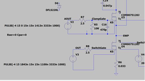
- Our C3M0075120J has pretty high internal RG (~ 9 Ohm), you need to use low external Rg to reduce the turn-off loss. Below gate drive circuit shows an example, and you will see significant loss reduction.
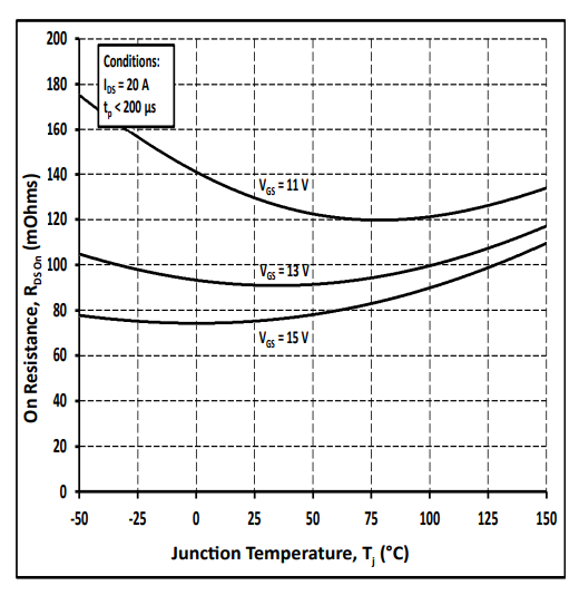
- With low turn-on voltage (+13V), you will have higher RDS_ON and conduction loss. Please refer to the following figure for the RDS_ON with different drive voltages. With 0V turn-off, the switch will turn off much slower with high turn-off loss as you can see from your simulation. Another note for 0V turn-off is that you may have false turn-on of the upper switch (so called "cross-talk") when the lower switch is turned on fast.
- In order to improve the heat dissipation, you can use thermal vias to take the heat out through the PCB and then to the heatsink. If you don't have space for the heatsink on the bottom of the PCB, then you need to use larger drain pad area and some metal fins for heat dissipation or something else which is possible. Whichever way you use, it is always good to reduce the power loss. You can try to use lower external Rg and negative turn off (-3V ~ -4V) voltage if you can with current circuit board and see if the thermal has been improved or not.
- Here are some good articles and videos on our websites which discuss the thermal solution for SMD and gate drive solutions. Hope they are helpful.
0 -
Hi, I hope that this answered your question. I will close this discussion for now but if you have a follow up question, please "Start a New Discussion" and we would be glad to support you further.
0


