
SpeedFit™ Design Simulator
Simulate and evaluate the performance of SiC-based power circuits and determine the right SiC device in seconds.
Start a SimulationCRD25DA12N-FMC PCB Design Related

We have couple clarifications related to the PCB design for the 25kW CRD25DA12N-FMC V1.1
- The hall sensor is oriented in such a way the input and output traces of the phase leg current paths are in zig zag as below . if the component was 180 shifted it would have been phase leg out to hall in , hall in to terminal and no need for criss crossing the power traces, any reason this approach was chosen
Hall sensor output to J17
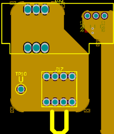
Phase leg output to hall sensor
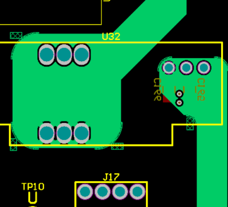
Making this 180 degree shift (U32) makes a clean connection path easier . curios any constraint prevented this hall sensor position ?
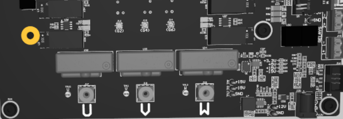
2. Why are all the 4 mounting holes for SiC Module Heatsink (and the 4 pcb mounting as well) done as gold plated through hole instead of regualr mouting hole only, they are very close to the vicinity of parts and can become a stub through the heatsink
Comments
-
Hi, I hope that this answered your question. I will close this discussion for now but if you have a follow up question, please "Start a New Discussion" and we would be glad to support you further.
0