
SpeedFit™ Design Simulator
Simulate and evaluate the performance of SiC-based power circuits and determine the right SiC device in seconds.
Start a SimulationI need the PCB layout footprint file and symbol of the CAB425M12XM3 to electrical CAD (EAGLE).

If it is possible, please send me also via the private message feature.
Thank you in advance for your help!
Zoltan
Comments
-
Thank you for your post, it has been approved and we will respond as soon as possible.
0 -
Hi Zoltan,
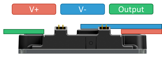
We do not have a PCB footprint available for EAGLE, but our design files for the KIT-CRD-CIL12N-XM3 contain the layout Gerber files that you can reference to create a footprint based on our recommendations. In order to connect the V+ and Midpoint terminals of the XM3 module to a PCB, you will need to fabricate metal standoffs that fill the space between the power terminals and the PCB. This is necessary as the power terminals of the XM3 module are not planar (to enable simple laminated bussing designs for minimizing inductance and cost) as shown below. Please find the recommended standoff design below.
Best Regards,
Austin C.
0 -
Hi,
Thanks for your help!
Regards,
Zoltan
0 -
Hi, I hope that this answered your question. I will close this discussion for now but if you have a follow up question, please "Start a New Discussion" and we would be glad to support you further.
0