
SpeedFit™ Design Simulator
Simulate and evaluate the performance of SiC-based power circuits and determine the right SiC device in seconds.
Start a SimulationCAB006M12GM3 gate driver layout in parallel and NTC connections

We are designing 2 level Active Front End with CAB006M12GM3. 2 modules per phase are connected in parallel.
- As per application note PRD-08911, Section 5.2 Power Layout Design, gate loops and power loops should not overlap. Is it ok to overlap gate drive loop of high side with DC planes. As DC plane voltages are constant, so dV/dt is negligible and hence capacitive coupling should not create issue? Does high dI/dt magnetic coupling create problem for gate drive?
- Single driver with isolated analog sensing is selected to drive paralleled modules, is it ok connect NTC of 1 module to high side gate driver and NTC of another paralleled module to low side gate driver? Will it create problem for isolation or noise?
Regards,
Jitendra
Comments
-
Thank you for your post, it has been approved and we will respond as soon as possible.
0 -
Hello Jitendra,
As discussed in the indicated section of the PRD-08911, the ideal layout would be to have no overlap between the gate and power loops. However, in practice — when dealing with application-specific constraints — we recognize that this is not always achievable. In these cases, we still recommend limiting noise coupling through two primary methods: (1) route the gate signals over the DC planes instead of the AC terminals, and (2) route the gate signals perpendicular to the flow of current in the power planes. In your case, routing the gate signals over the DC planes should be fine. You should still follow best practices for gate driver design, when possible. Having long connections — and therefore high inductance — between the power module and the gate driver can result in undesirable dynamics, regardless of whether you have high coupling between the gate and power loops. PRD-09301 provides more information on best practices for gate driver design for SiC power modules.
The NTC sensor in the power module is isolated from the other voltages. However, in the unlikely case of a catastrophic failure in the module, a wire bond or other debris may bypass this isolation barrier to the NTC sensor. For this reason, Wolfspeed recommends having an additional isolation barrier for the NTC feedback measurement (which it sounds like you are already adopting through the use of the gate driver with isolated analog sensing). It should not be a problem connecting the different NTCs to the high and low side gate drivers. The time constant of an NTC measurement is very long compared to all the electrical signals, so the signal can be aggressively filtered without loss of information. It is noted that in some Wolfspeed documentation, you may see that Wolfspeed typically recommends attaching the NTC to the low-side gate driver. This recommendation is based on situations where the NTC feedback could be routed to either the high or low side positions, in which case you might get minor noise improvement due to the better reference voltage. However, in all these cases and in your design, the high-side switch position is still sufficient. Section 3.4 of PRD-09301 provides some additional guidance on NTC feedback in SiC gate drivers.
Thanks,
Chris N.
0 -
Dear Chris,
Thanks for the clear suggestions.
AN that you suggested, PRD-09311, is routing to PRD-09301. We are designing power supply with TI UCC14241-Q1 which has additional enable signal to optimize standby consumption. In PRD-09301, Section 3.8 on common mode choke, it is recommended to use common mode choke which provide high AC impedance to common mode signals. First, is it safe to assume that all common mode noise flows through power supply pins and not through signal pins? Second, having common mode choke only in supply pins may cause noise in logic signals and should need digital isolator to interface between controller ground and power supply ground.
Regards,
Jitendra
0 -
Hello Jitendra,
PRD-09301 is the correct document number. Thank you for identifying the typo. I will try to get it updated in my original post to avoid confusion for any future readers.
Unfortunately, it is not safe to assume that all common mode (CM) noise flows through the power supply unit (PSU). The CM currents will flow through all available paths across the isolation barrier. Wolfspeed recommends a CM choke on the PSU since it is often a susceptible component for problematic leakage currents. It is important that designers still recognize the signal path as a potential CM path.
I agree that adding a CM choke could cause more noise in the signal path. However, the barrier capacitance of the PSU is often one of the most susceptible routes for CM currents, so the CM choke mitigates this. Additionally, Wolfspeed still recommends including filtering on all the signal pins. Adding the CM choke does not mean abandoning adding filtering and best practice routing to the signal chain. Most gate driver integrated circuits (ICs) — including the one you are using — include an integrated isolation barrier which means you do not need to also add a digital isolator.
Thanks,
Chris N.
0 -
Dear Chris,
Thanks.
Can you also suggest filtering for differential mode noise coupling due to SiC switching? As the inverter PWM turns on, ADC performance degrades.
Regards,
Jitendra
0 -
Hello Jitendra,
Please note that my original post has been updated to show the correct document number. Thanks for identifying the typo.
Regarding your recent question, can you please elaborate on the ADC issues you are observing? Are you having issues with an ADC measurement at your controller? Is it an NTC measurement issue? If you provide more details about your issue, I can provide better assistance.
In general, you can improve issues related to noise by: (1) using high-isolation-rated gate driver ICs and isolation power supplies to limit leakage back to the controller; (2) using filtering on the gate driver signals; (3) using differential signaling to reduce noise susceptibility; and (4) following layout best practices to limit unintended coupling. Many of these concepts are discussed in more detail for gate drivers in PRD-09301. Again, if you provide additional details about your exact issue, I can provide better guidance.
Thanks,
Chris N.
0 -
Dear Chris,
Thanks.
I saw your original post and it looks good now.
My question is for the power supply which is common between controller and gate drivers. Currently we have IGBT based 2-level AFE in which control is implemented using external Sigma Delta ADC which has SPI interface between controller and ADC but facing noise issues in digital signals (single ended signals) between controller and external ADC. Issue is in both supply and signals. Integration of SiC will make condition even more worse and how to take care of it.
Regards,
Jitendra0 -
Hello Jitendra,
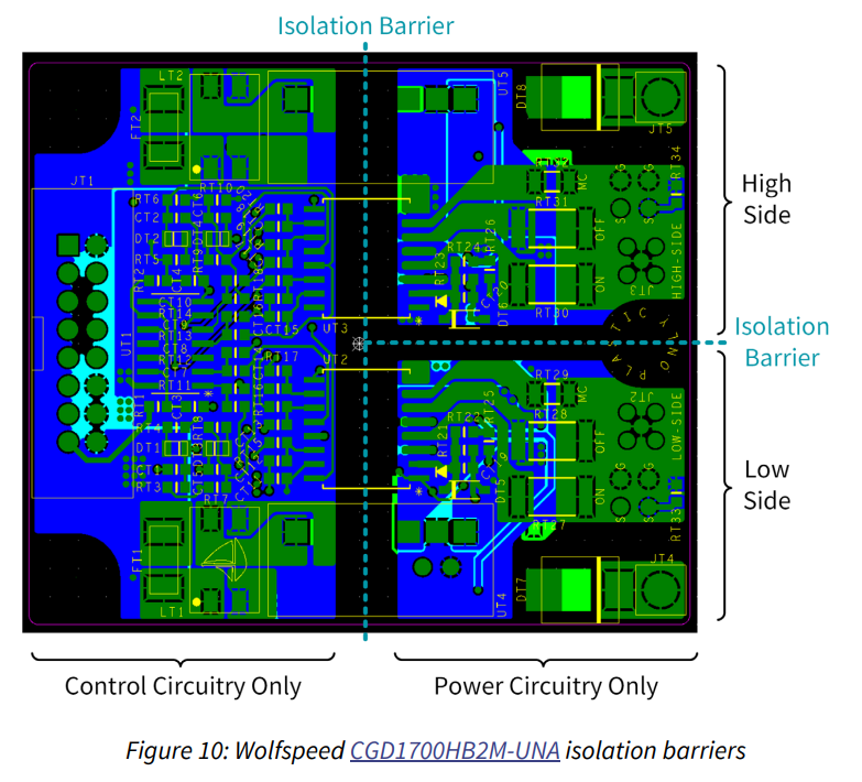
We recommend having isolation between the reference of the controller and the reference of the gate driver output. An example is shown in Figure 10 of PRD-09301 (repeated below). There is an isolation barrier between the control circuitry and the gate driver power circuitry. The only components which bridge the isolation barrier are the gate driver IC and the isolated DC/DC power supply. No copper on the circuit board bridges across the isolation barrier. If you are directly connecting the controller reference to the reference of the gate driver power circuitry, it could be the reason for your noise issue.
Do you have a picture of the setup? If you have a long connections between your gate drivers and the controller, you could further improve the robustness of the circuit by adopting differential signaling instead of single-ended. You could also add some filtering elements to the circuit and review your circuit board layout for potential areas which need better ground plane shielding or lower inductance routing.
Thanks,
Chris N.
0 -
Dear Chris,
Thanks for responding to all the questions.
- We are already using differential signalling as the connections are long
- Gate drivers and its power supply are isolated only. Still we are facing differential noise issue in the digital power supply of gate driver (which is used for digital side IOs).
- Yes, we should add filtering elements on digital power supply. I saw gate driver designs of Wolfspeed and was not able to conclude on what should be added for SiC switching. But this may be very specific to design environment. We will improve the layout also as you suggested.
Regards,
Jitendra
0 -
Hi Jitendra,
It sounds like you are already adopting several best practices. I'm glad to hear that you are using differential signaling since that improves signal immunity and that you are using both an isolated power supply and gate driver IC.
I recommend trying to keep your connections between the controller and your ADC as short as possible to limit noise susceptibility. Furthermore, high-precision analog measurements can be improved by limiting the overlap between analog signals and digital signals. If the return path of a digital signal is routed directly below an analog signal, it can introduce distortion into the analog signal. It is possible that you are having ADC issues independent of the power electronics. That is, just having high frequency digital control signals near your ADC measurement could introduce noise. Electromagnetic Compatibility Engineering by Henry Ott goes into some details about limiting this overlap.
It could be helpful to identify if the switching speeds of the power electronics is actually the cause of the noise. For troubleshooting, you could operate the power electronics at lower dV/dt by increasing the gate resistance. This would provide a better indicator that the power electronics are the root cause. Similarly, for troubleshooting, you could operate the controller + gate drivers without any MOSFETs and see if the noise is still observed. This may give an indicator if the controller layout is the root cause — independent of the power electronics.
Thanks,
Chris N.
0 -
Hi, I hope that this answered your question. I will close this discussion for now but if you have a follow up question, please "Start a New Discussion" and we would be glad to support you further.
0