
SpeedFit™ Design Simulator
Simulate and evaluate the performance of SiC-based power circuits and determine the right SiC device in seconds.
Start a SimulationRequest for DC Bus Bar and Bulk Capacitor Placement Guidance – CGD12HBXMP & CAB400M12XM3

Dear Wolfspeed Technical Team,
I am currently designing a high-power DC-DC converter and utilizing your CAB400M12XM3 power modules along with the CGD12HBXMP gate drivers. I would like to request your guidance regarding the optimal DC bus bar and DC bulk capacitor layout.
Due to space limitations in my mechanical design, the area available for placing the DC bus bars and bulk capacitors is quite constrained. I understand that minimizing stray inductance is critical for proper switching behavior, especially in fast-switching systems like SiC modules.
Specifically, I would appreciate your input on the following:
- Are there any recommended example layouts or mechanical guidelines for DC bus bar placement in conjunction with the CAB400M12XM3 module?
- Do you recommend a vertical stack arrangement for the +DC and −DC bus bars to reduce loop inductance?
- What would be your best practices for placing DC bulk capacitors in this context, especially in tight mechanical arrangements?
- If available, could you kindly share any reference designs, application notes, or mechanical drawings that illustrate an optimized DC bus bar and capacitor configuration for this module/driver combination?
Any advice, examples, or visual documentation would be extremely helpful as we move forward with mechanical integration and layout optimization. Thank you very much in advance for your support and expertise.
Best regards,
Pederas
Comments
-
Thank you for your post, it has been approved and we will respond as soon as possible.
0 -
Hello Pederas,
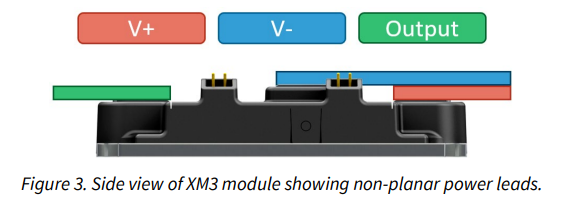
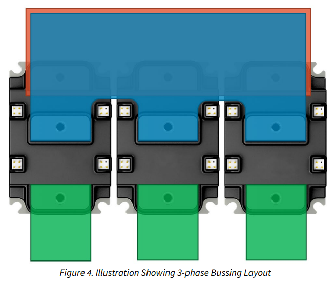
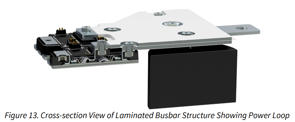
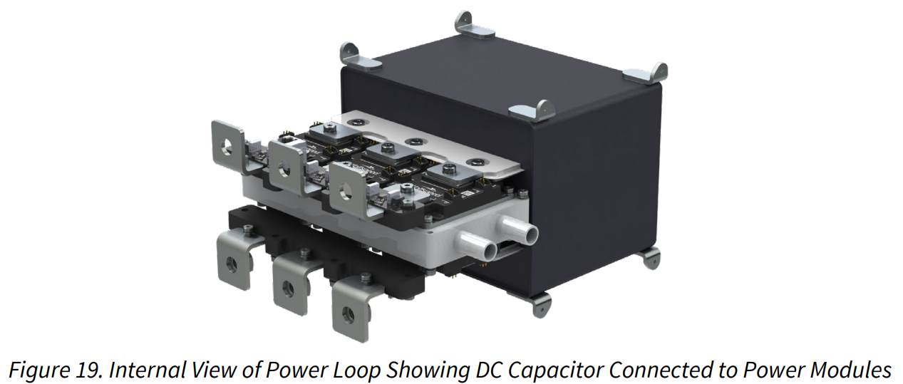
The CRD200DA12E-XM3 reference design uses the CAB400M12XM3 power module with bus bars and the CGD12HBXMP gate driver. It is a great example of how to implement bus bars in your design. The user guide (PRD-06975) for that design provides figures demonstrating the recommended approach for bussing the XM3 power modules. Additionally, the CRD600DA12E-XM3 reference design also uses XM3 power modules (in an alternative configuration); its user guide (PRD-06976) provides some alternative bussing strategies. I provided some sample pictures below from the guides, though I encourage you to review the entire user guides.
When designing your bus bars, we recommend that you adopt the following best practices:
- Ensure the DC+ and DC- layers are directly on top of one another to minimize inductance
- Place the bulk capacitors as close as possible to the modules to minimize inductance
- Do not overlap the AC outputs with the DC+/- layers to minimize coupling
Thanks,
Chris N.
0 -
Hi, I hope that this answered your question. I will close this discussion for now but if you have a follow up question, please "Start a New Discussion" and we would be glad to support you further.
0