
SpeedFit™ Design Simulator
Simulate and evaluate the performance of SiC-based power circuits and determine the right SiC device in seconds.
Start a Simulationshoot through issue

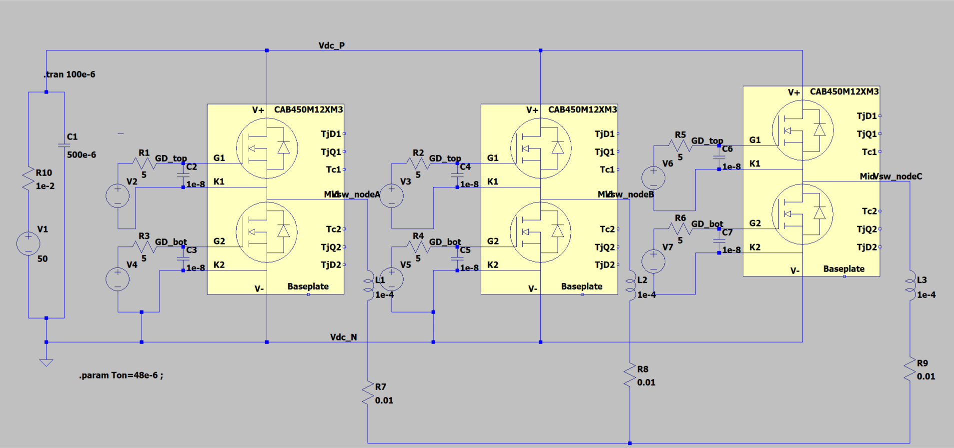
I am using CAB450M12XM3 for my inverter design. I have connected it with a 3 phase inductive load. I have applied a duty ratio of 48 us to all the top switches and 48 us to all the bottom switches with 2 us dead time. So it is like no load scenario for the inverter. But when the top switch is turning OFF, its antiparallel body diode is turning on during the dead time. Only when the bottom switch is commanded on then only the top switch body diode stops conducting which is causing a brief shoot through issue.
Comments
-
Thank you for your post, it has been approved and we will respond as soon as possible.
0 -
Please reply.
0 -
0
-
Hello Aradhya,
It is normal to experience switching loss even under no-load conditions as the output capacitance of the MOSFETs will charge and discharge when switching states. This phenomenon is actually utilized to discharge the DC link capacitor in some EV traction applications and is known as Active Discharge. I've attached a paper that explains the no-load loss mechanism.
Best Regards,
Austin C.
0 -
Thank you for the response.
But here I am not worried about the switching losses. If you see the results, it is clear that when the mosfet is turned off, its body diode starts conducting during the dead time. This is strange for me. I am not able to understand the valid reason. I need input on this. Please suggest.
0 -
Aradhya,
The current that you're observing in your simulation is not flowing through the body diode. This current is caused by the output capacitance of the device and is governed by i = C*dv/dt. You are creating a fast change in voltage across each MOSFET position (dv/dt), and the MOSFETs have an output capacitance (COSS), which causes a current to flow. I've added labels to your simulation result below:
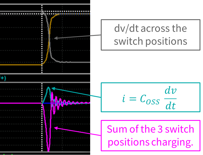
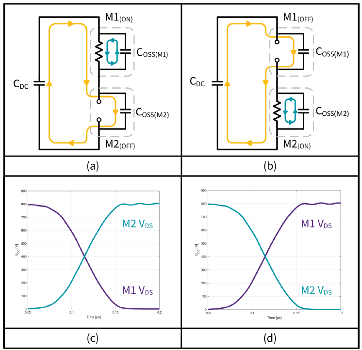
The paper in the post above walks through this phenomenon in more detail, but here's an excerpt showing the current path for high-side turn-on (a, c) and low-side turn-on (b, d). This paper is identical to your simulation where you're switching between the two zero states of SVM (switching between all high-side on and all low-side on simultaneously).
Best Regards,
Austin C.
0 -
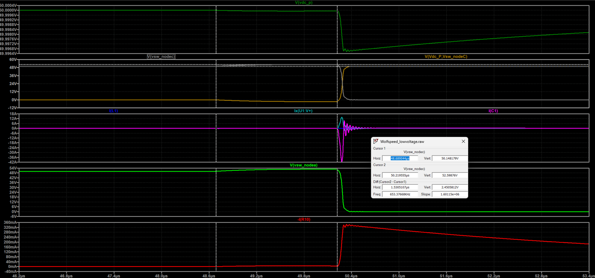
The above phenomena is happening after the dead time. But please observe the waveform during the deadtime. It can be observed that there is an increase in switch node voltage. The switch node voltage was equal to the DC link voltage when the lower device is OFF and upper device is ON. When the upper switch turns OFF, the switch node voltage is rising. I am concerned for that aspect. My query is also related to that. I am worried about the phenomena that is occurring during the dead time not after that.
 0
0 -
Hi Aradhya,
Thank you for the clarification; I'm following your question now. Can you please clarify the voltage setpoints for V2, V3, V4, V5, V6, and V7? Is the off-state voltage 0 V or -4 V for VGS?
Best Regards,
Austin C.
0 -
Hi Austin,
Thank you for understanding my query.The Gate voltage is 15 V during ON state and - 4 V during OFF state. It is same for all the switches.
0 -
Hi Aradhya,
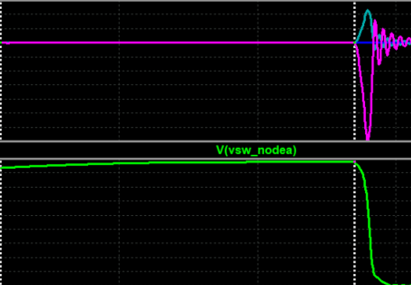
When the gate signal drops from 15V to -4V at 48µs during the turn-off event, we observe a rapid change in voltage (dv/dt) across the Cgd of the upper MOSFET. This change generates a current that flows through the circuit, affecting the Cgd, the gate driver, and the MOSFET channel. Consequently, a voltage drop occurs across the MOSFET, impacting the bus voltage and resulting in a higher voltage at the vsw_node.
I have attached a picture illustrating this behavior below. This behavior may be influenced by the floating model of the gate driver in LTspice. We are currently investigating this issue through hardware testing and will update you with our findings soon.
Regards
0 -
Hi Mhusian
Thank you for the response. But still it is not clear to me why the Vdg voltage will affect the switch node voltage.
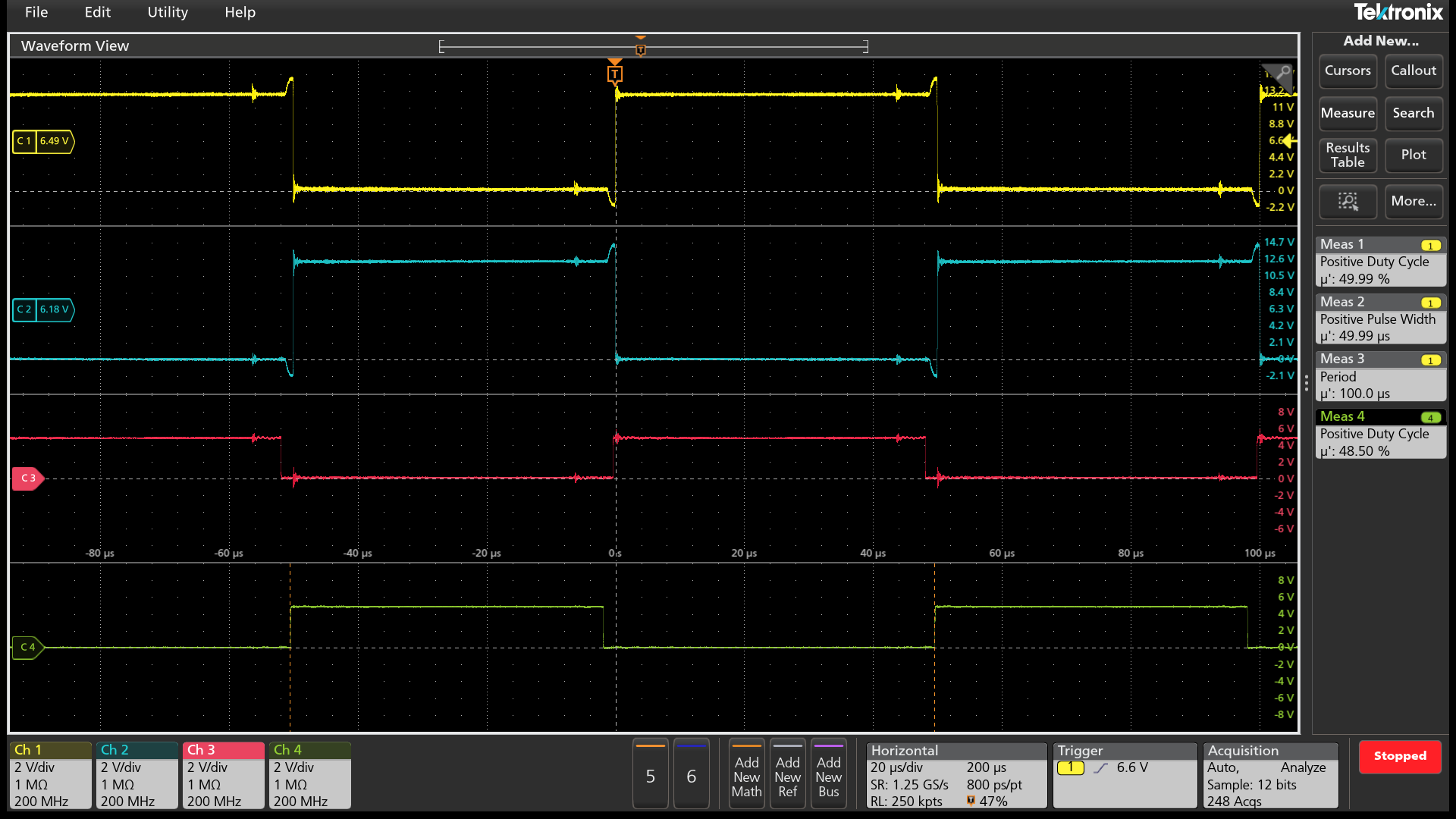
Moreover, I also have carried out the hardware testing and I have observed the same waveform. CH1 and CH2 refer to the VDS voltage waveform of Top and bottom switch. Here also there is a rise in switch node voltage during turn off scenario. CH3 and CH4 refers to the output from microcontroller to the gate driver circuit.
 0
0 -
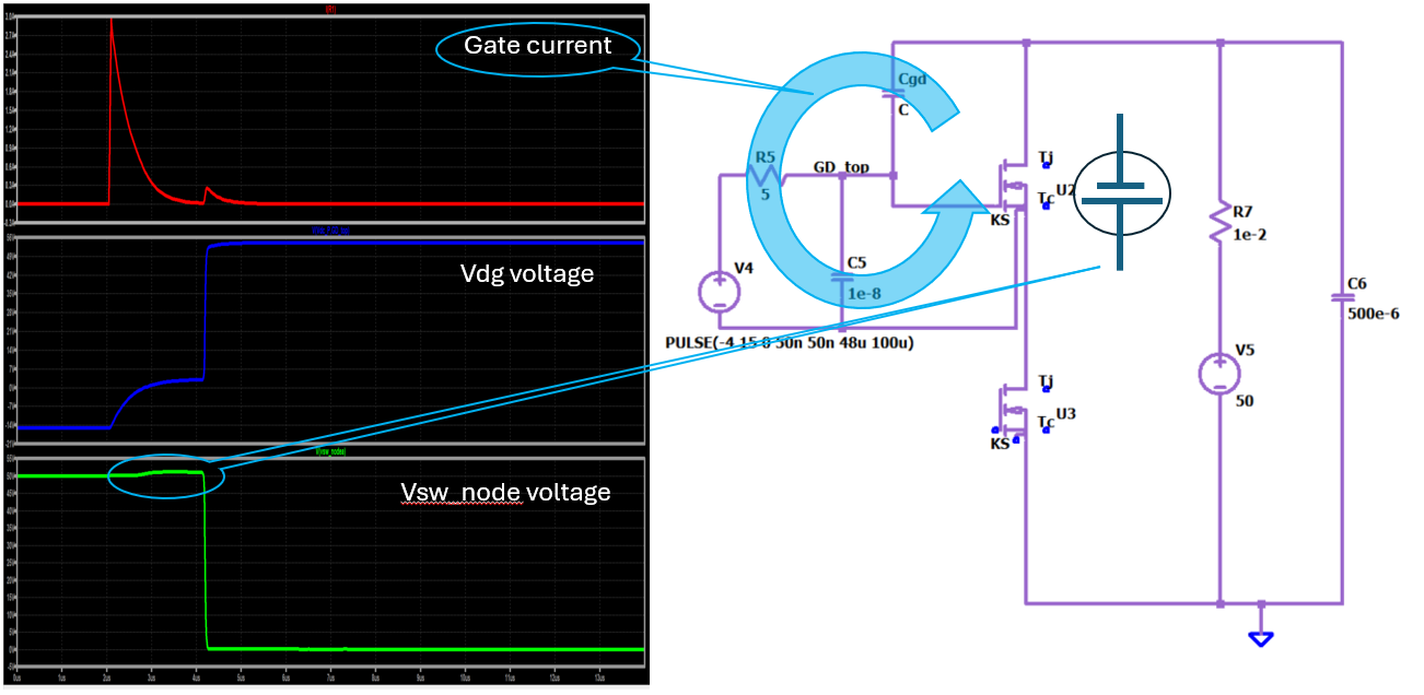
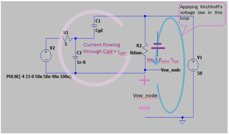
Hi Aradhya,
I’ve created a simplified schematic of the circuit to help explain this phenomenon. I've open-circuited the bottom MOSFET for clarity.
As I mentioned earlier, when there’s a change in voltage (dv/dt) across the gate-drain capacitance (Cgd), a current (Icgd) flows through it. This current travels through the gate driver circuit and back through the upper MOSFET. As a result, there’s a voltage drop across the upper switch, which can be expressed as
Vsd=Icgd×Rdson.If we apply Kirchhoff’s voltage law to the blue loop in the circuit, we can calculate the potential difference between the Vsw_node and ground. This gives us V(Vsw_node,ground)=V1(50V in this case)+Icgd×Rdson. The additional voltage drop (Icgd×Rdson) is what we observe as the rise in the Vsw_node.
I hope this explanation helps! Please feel free to reach out if you have any more questions.
Regards0 -
Hi Mhusian,
Thank you for your explanation.
The Cgd is initially positive when the top device is ON. While turning OFF, the Cgd has to go negative. The discharge current Icdg flows through the gate driver circuitry and the channel for which there is a rise in the switch node voltage.
But my query this charge rebalance should happen very quickly. However, I see this is going on till the dead time duration. What is the logic for that.
Moreover, is there any circuit arrangement to overcome this phenomena ?
0 -
Hi Aradhya,
Thank you for your message. During the transition when the switch turns off, the channel resistance increases, which blocks the voltage. This causes a longer time constant in the circuit where the Icgd is flowing, meaning that charge re-balance will take longer than what we expect.
I've attached a close-up image from the simulation showing the change in channel resistance of the upper switch.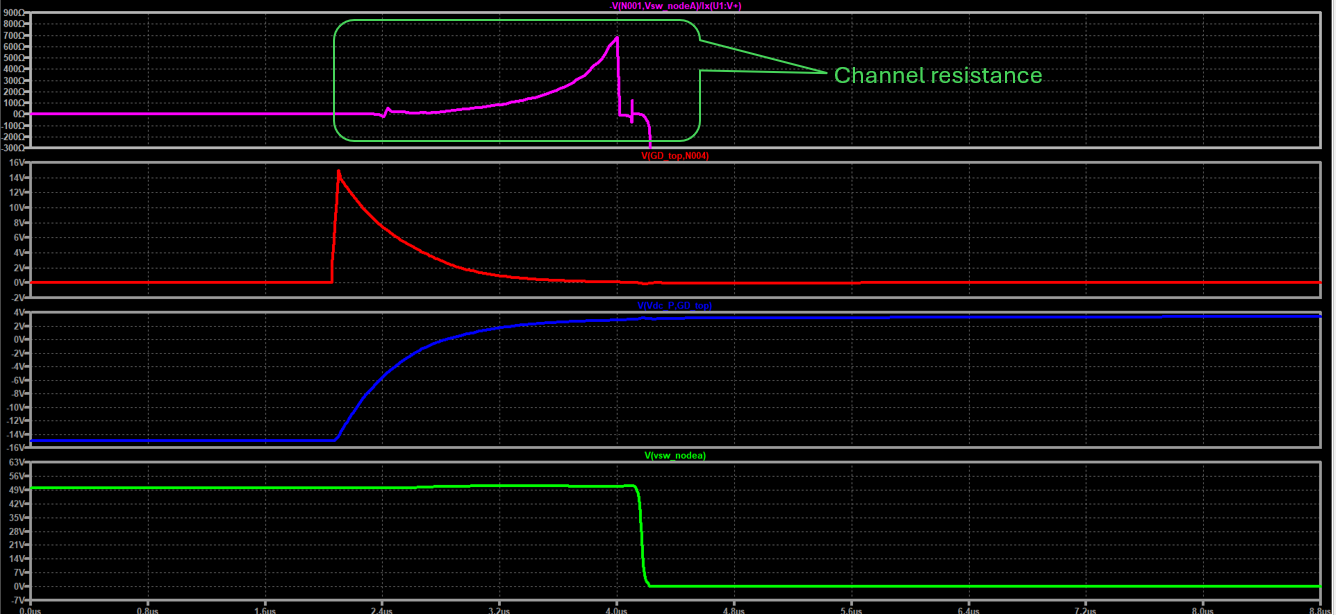
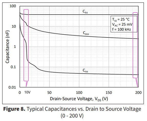
Additionally, increasing the bus voltage might help. As you know Crss is a non- linear function of Vds, so at low Vds, the Crss (Cgd) is significantly higher, leading to a longer time constant and slower discharge. In contrast, At higher bus voltages Crss is much smaller, resulting in a shorter time constant and faster discharge. I have also attached a the Crss Vs Vds graph for the module here for your reference.
If you have any further questions about this, please let us know!Regards
0 -
Hi Mhusain,
I agree the channel resistance is higher at low voltage. But I am observing this phenomena at no load condition even at higher voltage also.
0
