SpeedFit™ Design Simulator
Simulate and evaluate the performance of SiC-based power circuits and determine the right SiC device in seconds.
Start a SimulationCAB016M12FM3T ENIG vs Immersion Tin

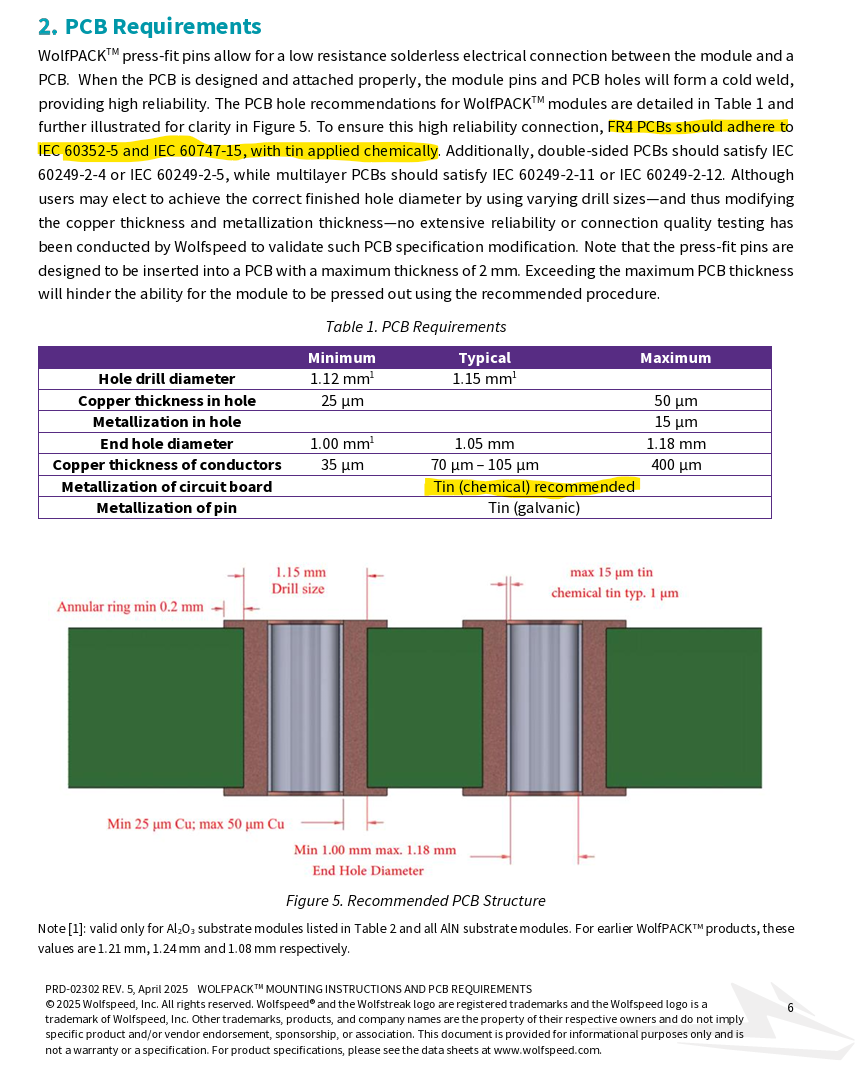
Immersion tin is shown as recommended for this PCB (attached photo),
but then goes on to say
"The PCB specifications provided in Table 1 are intended for immersion-tin surface finish PCBs. For guidance on ENIG PCBs please refer to the PCB specifications used in WolfPACKTM reference designs, such as the CRD25DA12N-FMC. Customers are advised not to specify the PCB press-fit holes solely by the end hole diameter. Even if the same end-hole diameter is achieved, achieving that diameter through a different combination of drill hole sizes and processes may not meet the specification. The specification provided to the PCB manufacturer should include all the information listed in Table 1, especially the drill diameter. Figure 6 depicts an example snapshot of the NC drill file shared with the board house where the press-fit pin holes are highlighted. This clearly tells the PCB manufacturer where to apply the specifications listed in Table 1."
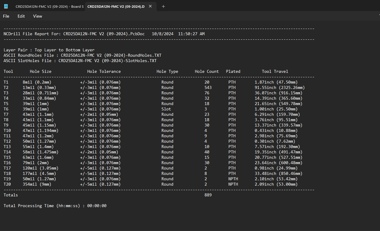
I found CRD25DA12N-FMC and found the attached information
in the files as well as the PCB design file (Altium). Do I follow those hole sizes for ENIG if I wish to do ENIG for the PCB fab? Looks to be 43.307 mil holes in the design and 60 mil copper around.
Comments
-
Thank you for your post, it has been approved and we will respond as soon as possible.
0 -
Hi Alex1234,
Thank you for reaching out. Wolfspeed's recommended guidance to include on the PCB Drill Table for ENIG plating is as follows:
THESE HOLES (1.09 MM +/- 0.065 MM) ARE FOR PRESS-FIT PART. USE 1.1811 MM +/- 0.025 MM DRILLED HOLES (SIZE 56 DRILL BIT). COPPER THICKNESS IN HOLE 0.025-0.05 MM. MAXIMUM METALLIZATION THICKNESS IN HOLE 0.015 MM.
Best Regards,
Austin C.
0 -
Thanks for the response. So if we use the part CAB016M12FM3T as press fit, can we still use that new guidance with ENIG or is that for soldering only? Would we still use the press fit jig?
0 -
Hi Alex,
Yes, this guidance applies to press-fit with ENIG plating. You will be able to use ENIG plating with the press-fit connection if you follow this guidance and order boards from a quality board supplier. Yes, you will definitely need a press-fit fixture and a press to assemble the boards & the modules.
Thanks,
Austin C.
0 -
@AustinC And there wouldn't be any corrosion issues with the material of these pins press fit with the ENIG finish on the PCB? Vs with the immersion tin finish on the PCB. Want to ensure there wouldn't be issues between the galvanic tin metallization of the press fit pins with the ENIG finish on the PCB.
0 -
Hi Alex,
The key advantage of the press-fit connection is the creation of a gas-tight contact interface between the pin and the PCB, which provides exceptional long-term reliability and strong resistance to corrosive environments.
For some additional background, all contact surfaces naturally accumulate oxide layers, organic residues (such as oils and grease), and other contaminants over time, which can negatively impact electrical performance and connection integrity. Among these, corrosion-induced oxide layers are often the primary cause of contact resistance and reliability issues for electrical connections with power modules. Press-fit connections address this challenge by applying sufficient contact force to mechanically penetrate and disrupt these oxide layers during the press-in process, which establishes a stable, low-resistance electrical connection. Also, for PCBs utilizing ENIG plating, we recommended that the PCB not be reused following a press-out process of the module as the integrity of the plated contact surfaces may be compromised.
Best Regards,
Austin C.
0 -
Hello Alex1234,
I hope that this answered your question. I will close this discussion for now but if you have a follow up question, please "Start a New Discussion" and we would be glad to support you further.
Thanks,
Chris N.
0