
SpeedFit™ Design Simulator
Simulate and evaluate the performance of SiC-based power circuits and determine the right SiC device in seconds.
Start a SimulationCAB5R0 SiC Power Module - Peak Gate Current and Gate Voltage Rise/Fall Times

Hello,
I just wanted to know what peak gate current and gate voltage rise/fall times were achieved in Wolfspeed's DPT of the CAB5R0 power module with zero external gate resistance for the product switching loss characterization. I'm asking because I would like to compare these numbers with what I'm achieving in my prototype so that I can get a fair idea how close the losses and switching performance will be compared to what Wolfspeed achieved.
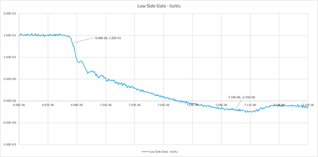
The images below show the scope captures of the gate current and voltage in my prototype:
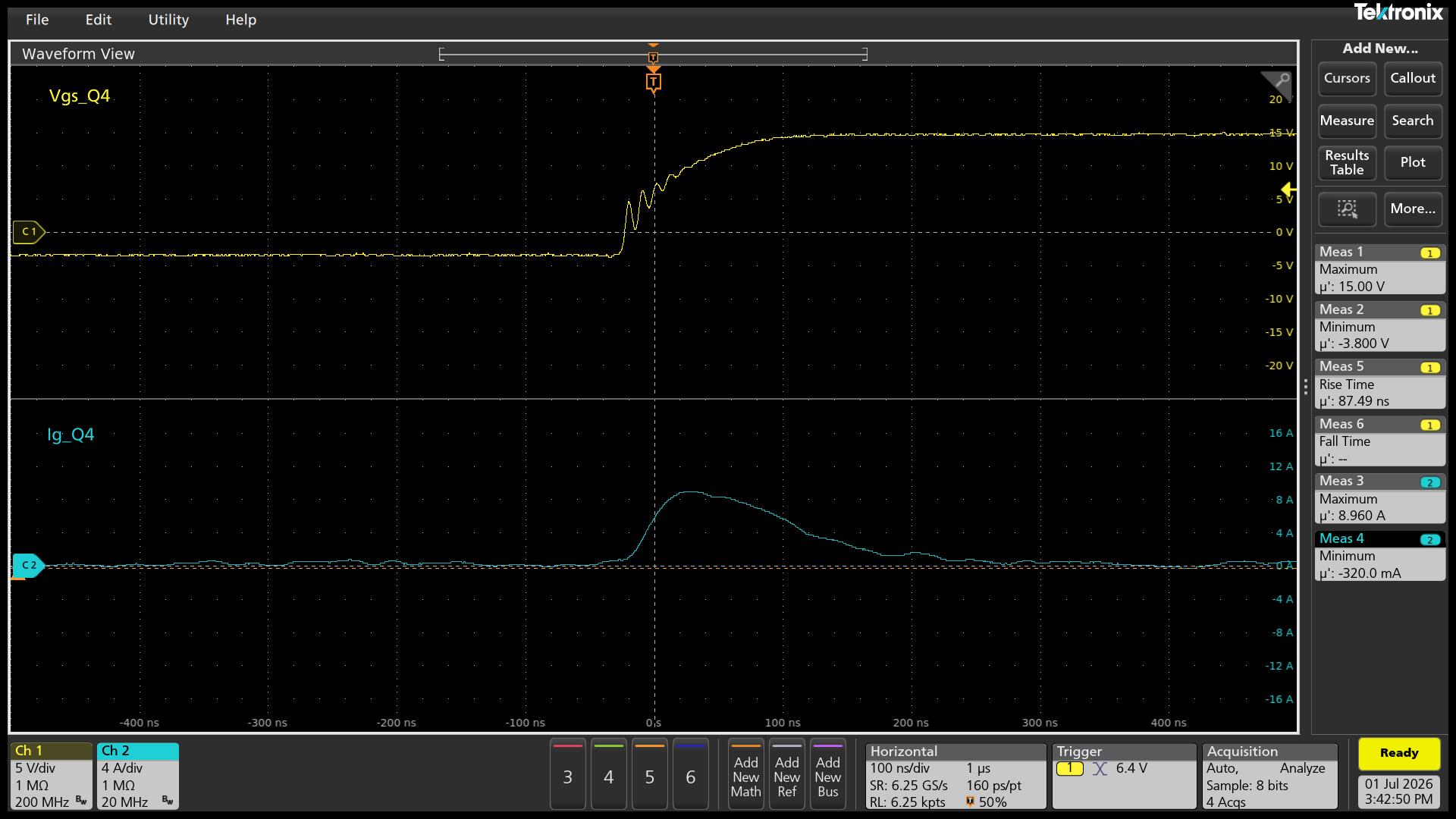
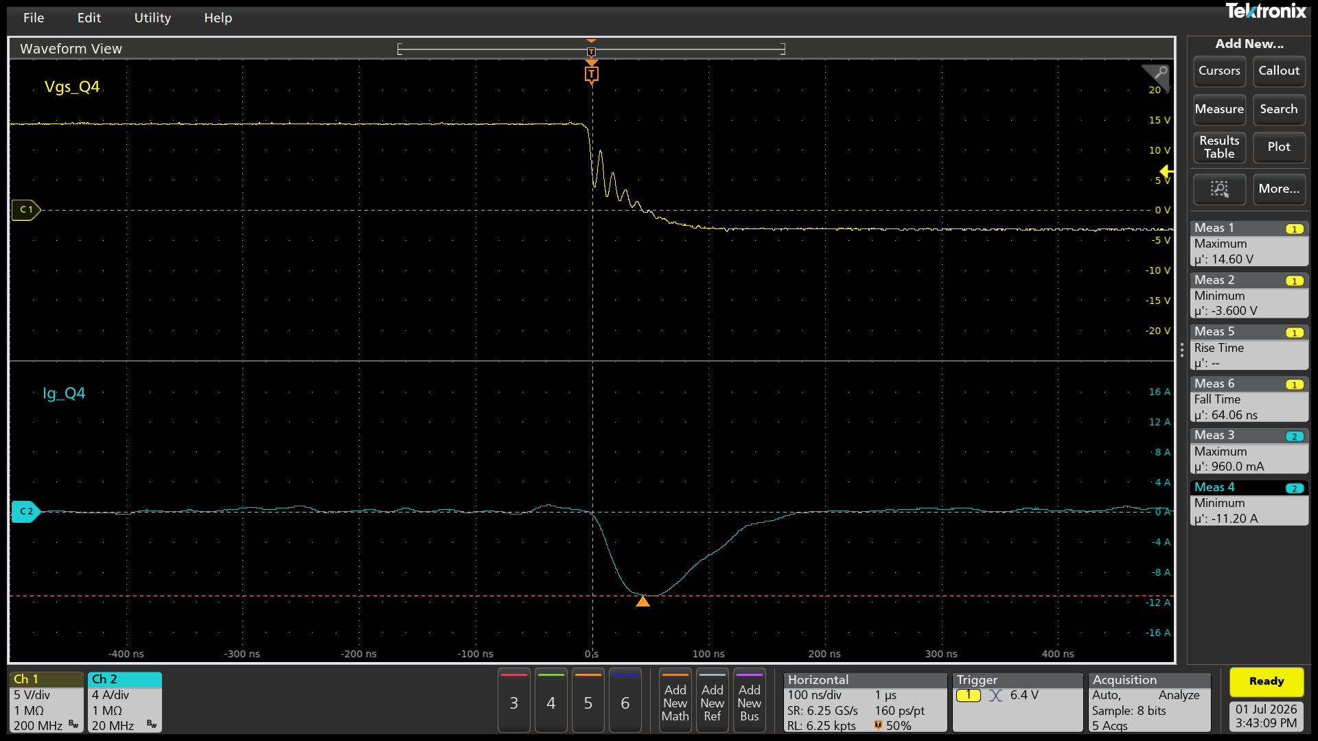
Theoretically, I calculated a peak gate current of ~17A, which I'm sure I can get closer to in a future revision of the board with some layout and design improvements, but as things stand, I would like to understand how close the losses and switching performance of the module will be to Wolfspeeds experiments.
Looking forward for your response.
Regards,
Prathik
Comments
-
Thank you for your post, it has been approved and we will respond as soon as possible.
0 -
Hello Prathik,
Please see the scope images from our testing of this device at 25°C, 1500 V and 240 A.
Turn On
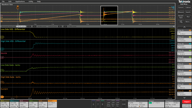
Looking at the raw data, you can see a rise time of 163 ns ( by 10 – 90% target voltage metric).
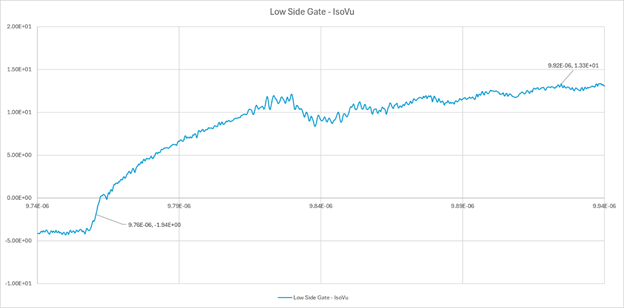
Turn Off
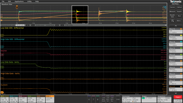
Looking at the raw data, you can see a fall time of 163 ns ( by 10 – 90% target voltage metric).
We don’t typically monitor the gate current when characterizing our devices but quantify the total gate charge and Ciss. This is reported on the datasheet.
By prototype design, do you mean a gate driver? Your design is using a higher current output gate driver IC than what we used if you are expecting an IGS of 17 A. We used the IXDD614SI gate driver IC as called out by the datasheet.
Are you operating with no bus voltage? If so, that will impact your results because gate capacitance will change with VDS. If you are switching with a load, could you provide your dV/dt results? That would be a better metric to compare the switching losses between your system and our measurements. This is because the rise/fall of the gate is not typically linear with time, and assuming you are hard-switching, dV/dt is a better predictor of switching losses.
Best regards,
Dustin
0 -
Hello Dustin,
By prototype design, I mean the DC-DC converter prototype that I have designed. I am using a gate driver with a peak drive strength of 16A (Not 17A, that was a typo. The precise peak Ig is 15.8A per calculations for 15V/-4V on/off state voltages and a 0.1ohm current sensing resistor).
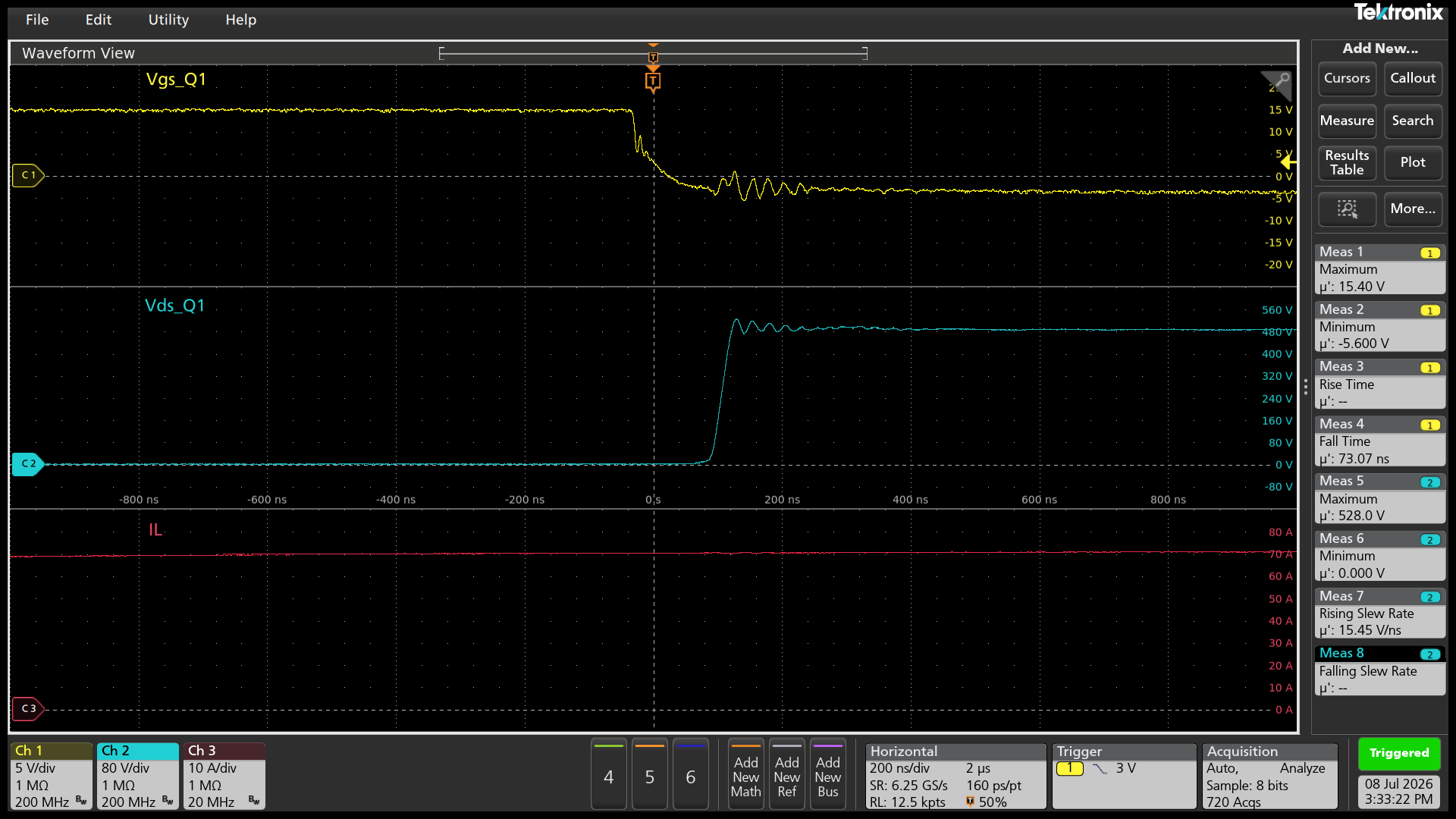
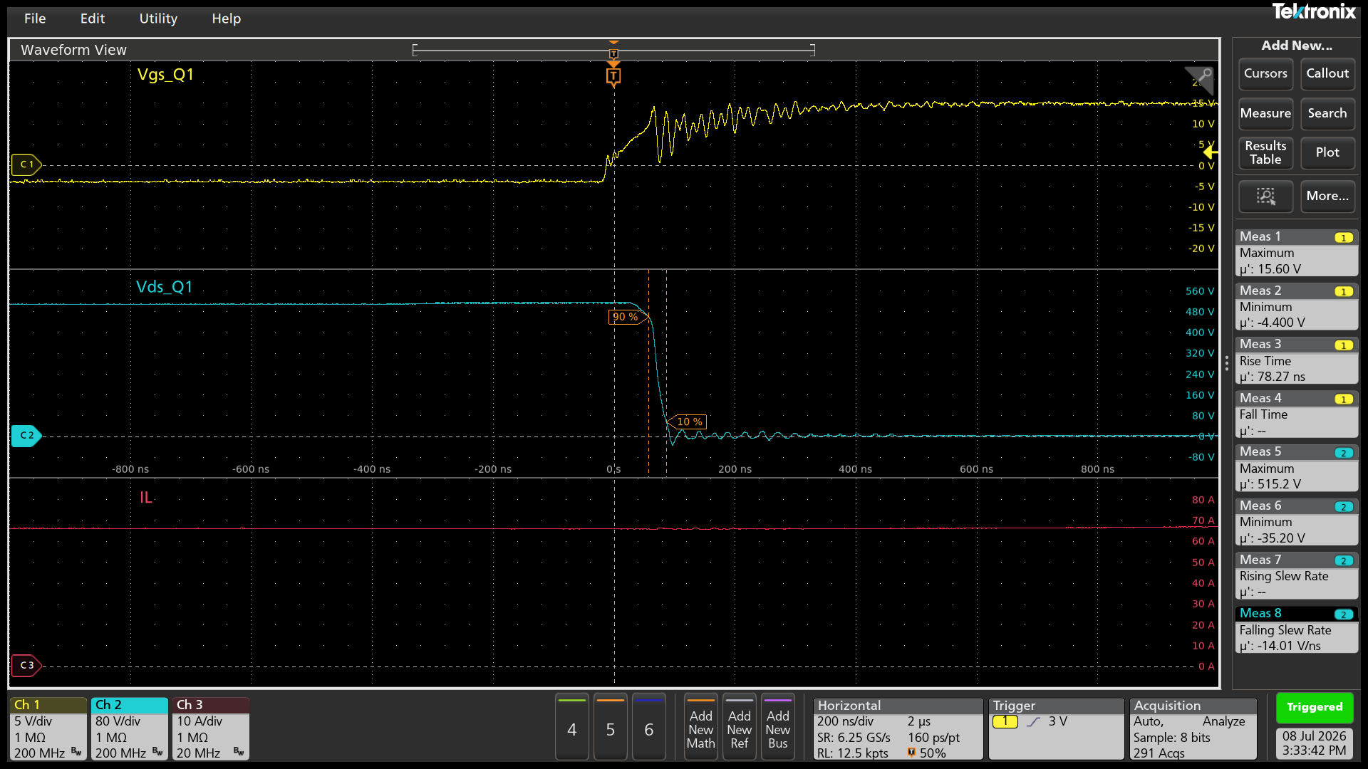
The gate voltage and current waveforms I uploaded are from initial tests with the converter powered off. Here are the scope images of the gate and drain voltage with the converter powered on at 500V and a load current of around 70A, hard-switched. Note that since my last post, I am using Rg_on = 1ohm and Rgoff = 0ohm.
Regards,
Prathik
0 -
Hello Prathik,
Thank you for sharing this additional information. The closest data point we have to your conditions is V_DC = 1200 V and I_DS = 80 A. Slew rates are based on the 10/90 calculation method you have used.
Parameters
Wolfspeed
Prathik
Ext R_G on/off (Ω)
0/0
1/0
T_J (°C)
25
Unknown
V_DC (V)
1200
500
I_DS (A)
80
70
Turn-On V_DS Slew (V/ns)
29
14
Turn-Off V_DS Slew (V/ns)
34
15
E_on
2.7
2.0*
E_off
0.8
0.8*
*Rough estimation based on linear scaling
If you plan on switching at a higher input bus voltage later, you can expect your V_DS slew rate to increase. For example, this module saw an 18% and 13% increase of V_DS slew rate for turn-on and turn-off, respectively, when moving from a 1200V to 1500V bus.
It does appear you are switching slower than our setup even considering the different bus voltages. My assumption is that your gate loop impedance is higher, and that your gate driver may have a higher internal R_G (the IXDD614SI gate driver IC we used has Rg on/off = 0.4Ω/0.3Ω).
0