
SpeedFit™ Design Simulator
Simulate and evaluate the performance of SiC-based power circuits and determine the right SiC device in seconds.
Start a SimulationParalleled SiC Mosfets, PCB Layout of Source Return Path when using Source Series Resistors

In APPLICATION NOTE PRD-06752, when paralleling discrete SiC mosfets , Section 2.3.5, "it is highly recommended to have resistors in the source return path as well. This limits current arising due to unidentical source inductance." Generally, I use mirrored planes for Gate/Source paths. When using source resistors, there is a break in the Source path from the Driver to the SiC KS pin across the resistors. There is no way around this, hence:
- Should you mirror the Gate/Source Plane from the Driver right up to SiC KS pin, including the Gate and Source Resistors?
- Should you mirror the Gate/Source Plane from the Driver up to the Gate and Source Resistors, and then from the SiC KS pin under the Gate and Source Resistors, where the plane gap is centered?
- What is the recommended Gate/Source plane mirror technique?
When there are no source series resistors the source from the Driver to the KS pin is the Source Plane is simple and contiguous. However, when using Source resistors is a break in the Source plane.
I would like to know the best layout practice to keep the Gate/Source path mirrored, with minimized EMI.
Any advice and recommendation is greatly appreciated.
Sincerely,
David
Comments
-
Thank you for your post, it has been approved and we will respond as soon as possible.
0 -
Hello David,
As you indicated, Gate/Source mirroring is critical for creating a low-inductance gate loop since it introduces flux cancellation (see PRD-09301 Section 2.2 for more detail). Regardless of whether a Source resistor is adopted, good mirroring between the Gate/Source connections with help with paralleling MOSFET since all the parallel MOSFETs will have a lower loop inductance. As with most engineering decisions, there is a trade-off when introducing a Source resistance since it also makes the Source mirroring more challenging.
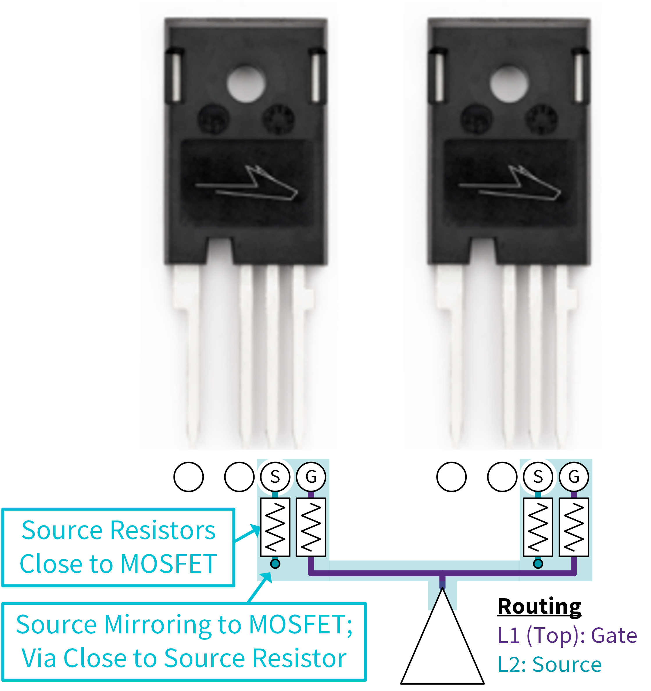
The recommendation is to place the Source resistor as close as possible to the MOSFET and maintain the Gate/Source mirroring all the way up to the MOSFET. The mirrored Source connection can still provide shielding and a high-frequency return path on the mirrored layer, even when including the Source resistor. This is shown notionally in the figure below.
In the figure, the gate driver output is centered between the gate pins on the top layer (L1) with short routing connections. The Source connection is mirrored below the Gate signal on Layer 2 (L2) using a copper pour; the Source copper pour is routed all the way to the Source terminal of the MOSFET, even though the actual electrical connection to the Source terminal is made through the resistor on L1. The board includes Source resistors close to the Source terminals of the MOSFETs. The Source resistors are connected through vias to the L2 copper pour as close to the resistors as possible, and the resistors are connected to the Source terminal through a short connection.
Thanks,
Chris N.0