Questions about CRD-02AD065N
Hello,
I came across your design: CRD-02AD065N that uses wolfspeed mosfets in bridgeless totempole PFC using Analog controller.
I am requesting the simulation file for that reference design since I'm unable to get it from the website.
Please he
Comments
-
Hello SJZ1 , our team is looking into your request and will post a response here shortly.
0 -
Hello,
Unfortunately we do not have a pre-existing simulation file to share for this reference design. You can use the documentation provided in the design files and SpeedFit to perform thermal simulations. If you would like to develop an offline PLECs or Spice model, all of our device models are available for download at:
Thank you for choosing Wolfspeed.
0 -
Hello,
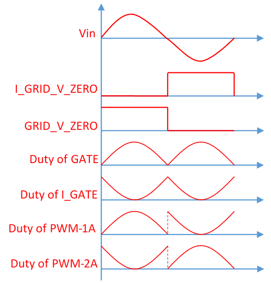
I would like to know how exactly this circuit is added for totempole operation, I understand that first it is sensing polarity of the input. But I am not clear about the Grid_V_zero and I_grid_V_Zero part and the arrangement of Logic Gates after it.
Also the ground for current sensing circuit that goes to the controller, is it to be connected with the same ground that connects return path from output capacitor to neutral(Vout_gnd)?
Looking forward to your reply
Thanks,
0 -
Answer to Question1: U1 is the PFC control chip, GATE is the output pulse signal, and I-GATE is its complementary signal of GATE. U3 is a comparator used to determine the polarity (positive or negative) of the input voltage. U5 is an inverter to obtain two complementary I_GRID_V_ZERO (positive half cycle is 0, negative half cycle is 1) and GRID_V_ZERO (positive half cycle is 1, negative half cycle is 0), both of which are 50Hz pulse square waves. In order to get the drive signals for the main switch and the freewheeling switch, U6, a "AND" logic chip, and U4, an "XOR" logic chip are used to achieve this function. The related waveforms are show as below.
Answer to Question2: The ground of the current sensing circuit and VOUT_GND cannot be tied together. The PGND of the current sampling in the main board and GND2 in the auxiliary power board are already connected. We used the DC output voltage signal as the input voltage of the auxiliary power supply board, which is isolated by a transformer. So the VOUT_GND of DC output shouldn’t be connected with PGND together.
0 -
Hello YuequanHu,
Firstly thanks for the reply.
I get how the inverter IC is used to get I_Grid_V after getting polarity from AC input.
I have tried to simulate the design in the Infineon simulator since the controller IC used in your reference design is from Infineon. To simplify the circuit I didn't include the controller IC yet and used a square wave source for PWM signals of MOS.
And the current sensing circuit is not included. This is how the circuit is looking:
and this is the result for circuit 1:
Then I added the Current sense circuit with grounds as connected in reference design pdf. (I have given different names to the ground but I don't know for sure if that helps)
This is how the circuit looked then:
And this is how the output looks:
As you can see, in the first circuit the inductor current is not in phase with input voltage and still has peaks
And in the second circuit, the current magnitude is not making sense along with undesired output voltage.
(Edit: if two different grounds are the problem here, what can be done to overcome that in simulation)
Can you help with which circuit/approach is more correct for simulation?
And what errors I am making in the circuit?
Awaiting your response.
Thanks in advance,
0 -
Attaching the report pdf file here that has clear schematics and waveforms:
Regards,
0 -
Thanks for the additional information, SJZ1
The engineer assigned to this post will respond shortly.
0 -
Dear Sajal,
In order to have correct operation and simulation results, the ground for current sensing and the power ground cannot have the same potential (voltage). If they have the same symbol they will have the same potential as defined by the simulation tool even if you use a different names.
You can give it a try first. If you still have problem, you may connect the two grounds using a large resistor (1M or larger).
We suggest using our Speedfit for evaluations of our parts because this will give you results in a few minutes.
Thanks.
0 -
Hi, I hope that this answered your question. If it did, please click on "This question has been answered - Close Discussion" . If you have a follow up question, at a later date, please "Start a New Discussion" and we would be glad to support you further.
0


